Fundamentals of High-Speed Design

Zachariah Peterson
|  Created: May 6, 2022  |  Updated: November 26, 2023

This track is for the designer who is new to high-speed layout and routing practices and wants to understand how they relate to signal integrity, and how to get started designing for high-speed digital applications.

Slides From Presentation

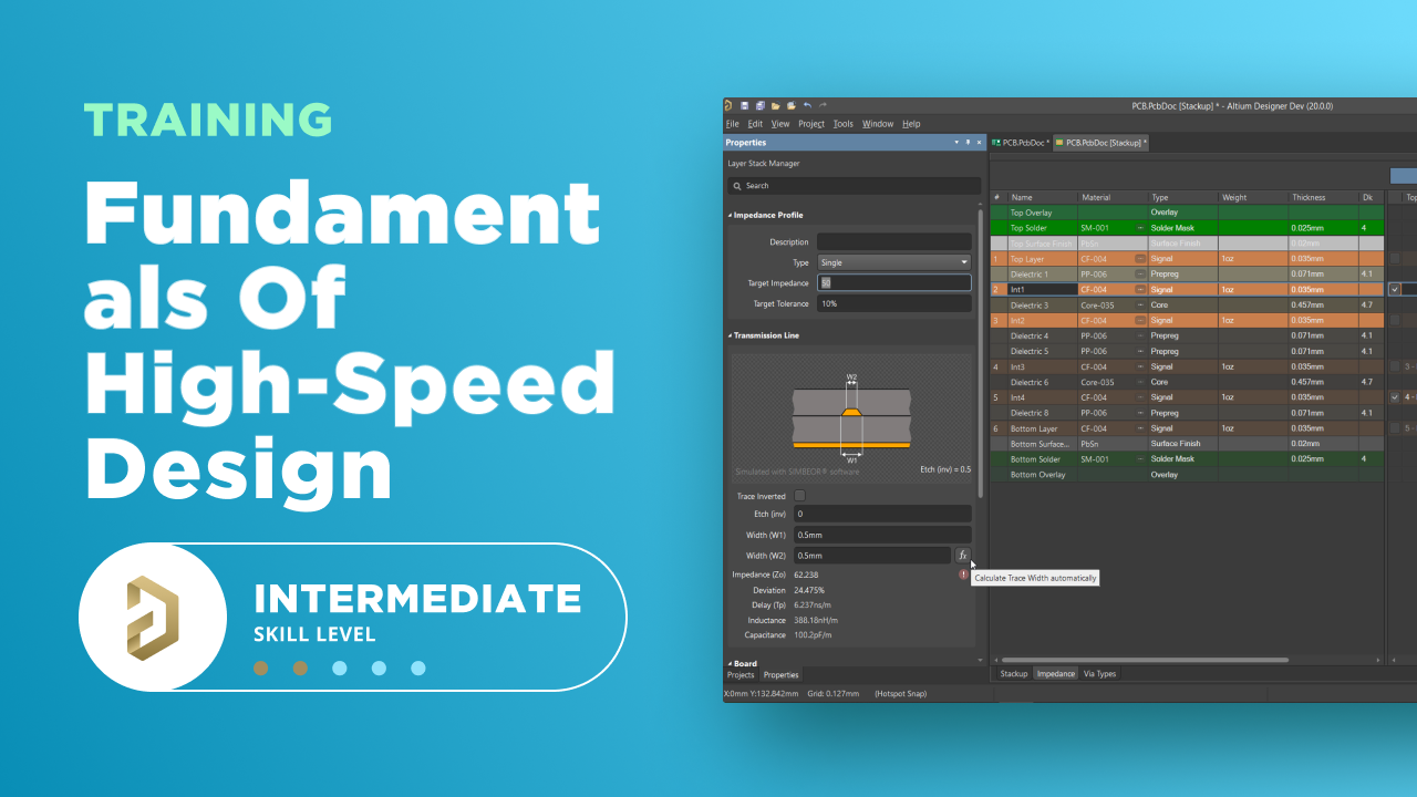
  • Stackups - material selection, planning the stack-up to support routing
  • How to design stack-ups to balance impedance, power, and ground
  • Different types of interconnects supported in Altium Designer, understanding impedance
  • Front-end planning and considerations during PCB layout/routing

About Author

About Author

Zachariah Peterson has an extensive technical background in academia and industry. He currently provides research, design, and marketing services to companies in the electronics industry. Prior to working in the PCB industry, he taught at Portland State University and conducted research on random laser theory, materials, and stability. His background in scientific research spans topics in nanoparticle lasers, electronic and optoelectronic semiconductor devices, environmental sensors, and stochastics. His work has been published in over a dozen peer-reviewed journals and conference proceedings, and he has written 2500+ technical articles on PCB design for a number of companies. He is a member of IEEE Photonics Society, IEEE Electronics Packaging Society, American Physical Society, and the Printed Circuit Engineering Association (PCEA). He previously served as a voting member on the INCITS Quantum Computing Technical Advisory Committee working on technical standards for quantum electronics, and he currently serves on the IEEE P3186 Working Group focused on Port Interface Representing Photonic Signals Using SPICE-class Circuit Simulators.

Related Resources

Related Technical Documentation

Back to Home