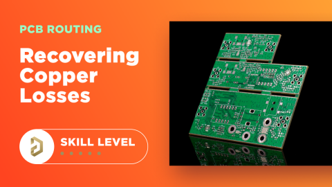
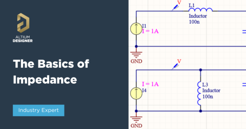
Meeting Standards: IPC 6012 Class 3 Via Sizes and Annular Rings Take a look at the above image of a PCB layout, specifically the vias and drill holes poking through the silkscreen. It's quite clear that some of these vias are off-center, meaning the drill hit that created these vias was not dead-center in the receiving land. This leaves behind an annular ring, something which might be considered a defect in certain IPC product classes. Under the IPC standards for rigid boards, we have several possible Read Article When to Use Tented Vias in Your PCB Layout Some designers swear by tented vias and prefer to always use them. When should these be used and when should they be avoided? We’ll explore in this article. Read Article Design Your Electronic Device with Hacking in Mind A very eye-opening world of hacking and understanding the never-ending risk to secure your electronic device. You wouldn’t want to miss this episode with a famous “good hacker” Joe grand. Watch now or listen on the go. Read Article SAP (Semi-Additive PCB Process) – How Creative Can You Be? Challenge how creative you can be! Can SAP processes produce plated through vias? Read this article to find out! Read Article PCB Design - Fun, Frustration and Misconception What do the top minds in the PCB Design social media space think about the modern landscape? We sat down with Hacksmith Industries, DD ElectroTech, and Electgpl to chat about how they got started, what frustrates them, what they think about A.I., and much more. Chris Thiele - Hacksmith Entertainment Ltd. So I think the most challenging design I've ever made was a Daft Punk helmet, Guy-Manuel. I designed several boards for that project, and they Read Article How to Choose Board Plating and Thickness for Your PCB Ever wondered what surface plating you should use? We've compiled important data on PCB plating. Read Article What's HDI? Design Basics and the HDI PCB Manufacturing Process Learn about design basics for HDI PCB board design. When planning for the HDI PCB manufacturing process, you can prepare accurate designs and deliverables with Altium Designer. Read Article Recover Conductor Losses By Clearing Your PCB Ground Layer Need to recover some conductor losses? Here’s how clearing out your ground plane near an I/O or connector can help. Read Article Pathological Design Features: Eric Bogatin on PCB Design Our podcast all-time favorite podcast guest is back to help PCB designers recognize bad PCB design guidelines. Tune in and listen on the go now. Read Article All About PCB-Mount Transformers Before you rectify your AC input down to DC, you’ll need to step down your mains power to the desired voltage with a PCB-mount transformer. Read Article Everything You Need To Know About Impedance Is understanding impedance really complicated? Expert Tuomas Heikkila will walk us through the basics of impedance. In this article, you will learn where impedance originated which will help you when designing your PCB or electronic projects. Read Article What is the PCB Supply Chain? The PCB supply chain encompasses all portions of PCB manufacturing processes, reaching from raw materials to components. Learn more about the PCB supply chain in our guide. Read Article Designing a Home Automation IoT Device In this article Ari Mahpour walks you through how to create your own IoT connected device and control other smart home products. Read Article OnTrack Newsletter: Altium and IPC form Partnership, Fab Notes and Food for your Brain - November 2021 November 2021 VOL. 5 No. 5 Full Article | Watch Video | Brain Food IPC joins Altium as Newest Nexar Ecosystem Partner Recently IPC and Altium formally announced that IPC is joining the growing body of the Nexar ecosystem. In this interview, we talk to David Bergman, VP of standards and technology at IPC. He talks about how he thinks this new partnership will bring bi-directional value to both organizations. Read Full Article What's In PCB Read Article How to Design to a Differential Impedance Specification Differential impedance is sometimes misunderstood and it depends on multiple factors. Learn more about trace width design needed to reach a specific differential impedance target. Read Article The NEXAR Ecosystem Zach chats with Altium's Vice President Lawrence Romine about the exciting future of PCB Design. Listen to this episode to learn more about Altium's mission. Read Article Is It Printed or a Component? All About PCB Test Points A PCB test point can be a simple pad in the PCB layout, or it can be a specific component where you can connect a probe. Read Article Pagination First page « First Previous page ‹‹ Page35 Current page36 Page37 Page38 Page39 Page40 Next page ›› Last page Last » Load More