
The PCB layer stackup you build to support high-speed board design needs to be engineered based on layer counts, layer thicknesses, and component lead size.
A TVS diode can help with your PCB layout withstand an ESD event by diverting surges away from protected components.
Transmission line taper structures can provide superior impedance matching between two transmission lines with approximately real impedance.
In this blog, Phil Salmony offers beginner PCB design engineers a good starting point to understanding vias. We will tackle the basics and recommended parameters. Read now to learn more.
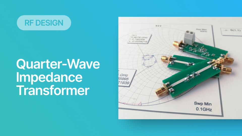
All quarter-wavelength transformers can be used for real loads, but some can be used for reactive loads with an additional transmission line section.
Your BGA fanout strategy depends on the BGA pad size and your pin density. Learn how to pair the right BGA pad size with PCB trace width in this article.
To readers who have been working in the PCB industry for most of your career, you have probably seen a