


Today's PCB Designers Are Driving Electronics Product Design

At a Glance
PCB designers don’t just build boards and assemblies. Today, they are mainstays in the electronics product design process.


Professional designers know they play a fundamental role in the electronics product development process. Without circuit boards, all those semiconductors are a bit meaningless, and they would not be able to provide the modern experiences we all enjoy. Even as PCB designers are so critical in the product development process, they still get the short end of the stick when it comes to product development tools. PCB design software is great for building a physical layout, but the capabilities have been slow to expand into a full product development suite.
What can the industry do to support PCB designers as they continue taking a more active role in product development? Here at Altium, there has been a progressive shift towards looking at the system level and creating tools that get designers more involved throughout the product development process. As the saying goes, over the wall engineering is over… today’s most successful products are built in a collaborative process.
What’s Involved in Electronics Product Design Beyond PCBs?
The very idea of product design should be obvious: it’s about considering the entire system in totality, and goals are accomplished by engineering the relationships between the major components in the system. For example, the enclosure and HMI elements drive placement on the PCB and component selection for EEs, the number of boards and connectors drive harness needs, simulation results can influence how the assembly is arranged and selected materials… the list of possible engineered relationships in a system can obviously be very long.
The Enclosure
Although the PCB and its components are responsible for creating a desired user experience, the enclosure is what the user will interact with. So of course, the enclosure has to make the user experience accessible, and it needs to have a pleasing aesthetic. It also needs to house all of the components and subsystems in a single package, and this simple requirement starts to put serious constraints on the PCB layout.

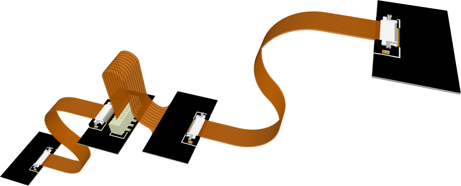
Multiboard Systems in Electronics Product Design
Fewer products are relying on a single board or component, and many products will not stay static throughout their lifecycle. Many products rely on multiple components and subsystems, including multiple PCBs that must connect to each other electrically and mechanically. In MCAD applications, mechanical designers have two approaches to working with their ECAD collaborators.
The old way: export each board as a STEP model, share/email these to the MCAD user, then they are imported into an MCAD application for mechanical backchecks.
The new way: Integrated ECAD/MCAD collaboration, where the MCAD user can access all boards as a single system without file exports.
We still see this happening in many companies, where the electrical and mechanical designer have to export files for each other in order to have visibility of the mechanical design for a product. Altium 365 has confronted this problem by provisioning the MCAD CoDesigner extension through the cloud so that MCAD and ECAD users can collaborate directly through a secure online platform.
The new approach is to apply logical definitions between boards and visualize mechanical constraints in the PCB CAD tool. ECAD/MCAD collaboration, where the mechanical and electrical design software are integrated, handles the mechanical collaboration aspect. Logical definitions between different boards is something totally new that requires cable and harness design, both in the schematics and in the PCB layout.
Cable and Wiring Harness Design
When you have multiple boards in an assembly, they need to be connected to each other electrically and mechanically. Wiring harnesses and cables are the standard components used to connect multiple boards in an assembly. While wiring can be mechanically simulated and visualized in 3D, these connections are rarely defined logically in the schematics. This means there is no net connectivity checking across cables, and the electrical designer can’t take advantage of many electrical simulation and verification tools required for full product evaluation without an external modeling application.
With logical definitions now being incorporated in the schematics, users can verify net connectivity in the PCB layout based on the logical definition in the schematic editor. For advanced products with multiple boards and components, this brings a new dimension to rules-based design inside an ECAD tool. The logical definition for a harness does not change its role as a mechanical element in a PCB layout, and the entire assembly can be used in an MCAD application as part of the mechanical design.
Electronics Product Designs and Devices: Power and EMI
Any electronic device that will be produced and sold en masse must pass emissions testing and receive certification to be considered compliant. For advanced electronic product designs with many digital subsystems, the relationship between power and EMI are a particular pain point. Unstable power delivery leads to radiated and conducted EMI, and identification of this needs to be brought earlier into the design process.
PCB designers need to have access to simulation tools inside their PCB design software that can streamline the model creation process, as well as iteration and optimization. Historically, simulation suffered the same inefficiencies as working with MCAD users: it required model exports, and then someone with a PhD in computational electromagnetics needed to create a numerical model of the design in order to run simulations.
Access to simulation capabilities to diagnose power problems should happen right inside the PCB layout. PDN analysis tools have been around for some time, but the newest generations of tools do not require users to leave their PCB editor. Instead, a product design process requires quicker iteration without relying on slower system-level simulations:
- Working in the layout, the designer can identify many simple power problems quickly
- These can be corrected inside the PCB layout without a model export
- Once full system evaluation is needed, a model is exported and given to a simulation engineer
To help users stay productive, EDA tools need more of this integration directly in the PCB editor. The new Power Analyzer tool in Altium Designer provides exactly these capabilities to help product development teams streamline their evaluation and optimization workflow.

Collaboration and Teamwork in Electronics Product Design
For product development to work successfully, everyone needs to have collaboration tools that streamline communication. Here are just some of the features product development teams need:
- Task management and assignments to team members
- Difference compare and merge features that integrate with version control
- Commenting throughout design documentation
- Access to component data in a secure cloud platform
Commenting features throughout PCB design documentation brings collaboration all the way through the product development process and into the production phase.
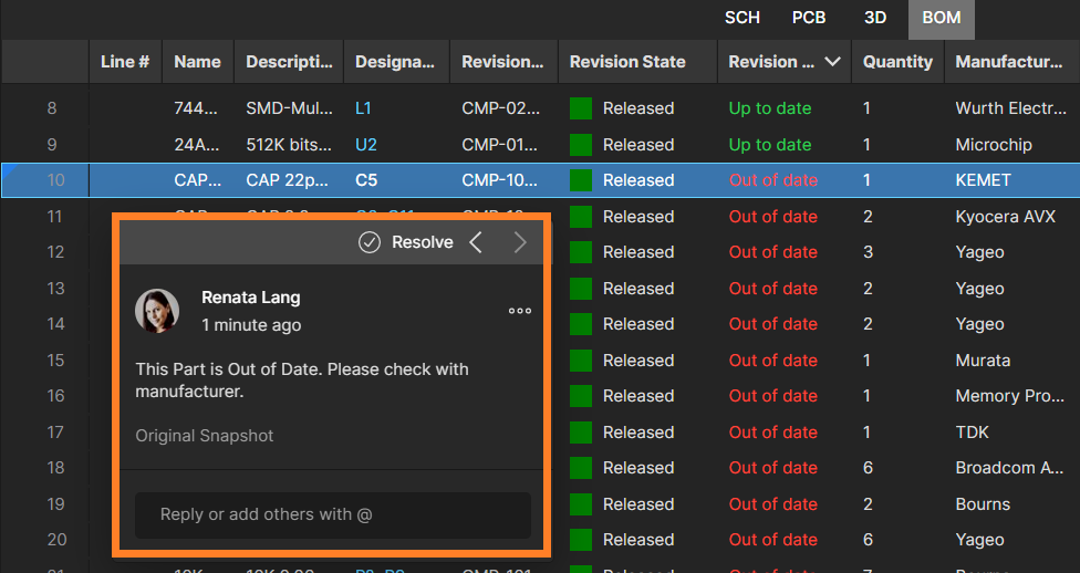
Designers building advanced technologies can take advantage of the industry’s best electronics product design development features in the newest version of Altium Designer®. Team members can collaborate, share design data, and create streamlined design processes using the Altium 365 platform. Come see the newest feature releases in Altium Designer.
We have only scratched the surface of what’s possible with Altium Designer combined with Altium 365. Ready to experience a truly unified electronics product design environment? Start your free trial of Altium Designer and discover how extensions and the Altium 365 application suite can help you work smarter, not harder.

About Author
Related Resources
Table of Contents
Design to Release, Without the Friction
- Keep reviews tied to the right version
- Reduce handoff confusion and rework
- Spot sourcing and release risk earlier
- Work solo, share when needed
Get Started
Thank you, you are now subscribed to updates.


