


El desafío del diseño de apilado de PCB de alta velocidad

At a Glance
Los apilamientos para PCBs de alta velocidad pueden diseñarse de muchas maneras, pero estos sistemas deben construirse equilibrando las restricciones de ingeniería en un producto final.


Although we would like to build every high-speed PCB perfectly, with ideal SI/PI/EMI characteristics, it is not always possible due to many practical constraints. Sometimes a stackup can be "good enough" even for a high-speed PCB. This always arises from the need to balance engineering constraints, functional requirements, and the need to ensure signal and power integrity in a high-speed design, and finally to ensure compliance with EMC requirements.
Even with all the good guidelines out there for high-speed design, there are particular aspects of stackup construction and its relationship to board construction that are often overlooked. My goal here is to go beyond the typical SI/PI guidelines and look at these issues from a more engineering perspective. When I say "engineering perspective," I'm referring to all the other constraints in a product that drive board design.
Translating Product Constraints into Stacking Needs
If we start from an engineering perspective, we should begin by developing a list of constraints and functional requirements for the system we want to build. On a high-speed PCB, we typically start with a particular component we want to use. When working on client projects, this will almost always be a specific processor and its peripherals (CPU or FPGA, memory, other specialized chips, etc.). An example of a list of constraints that might apply in a typical high-speed PCB design includes:
- Number of main component pins and pin size (e.g. BGA)
- Number of I/Os on large components, which determines the number of layers
- Number of interfaces, as well as the number of signals on each interface
- Target plate thickness, which may or may not be standard thickness (62 mils)
- Loss target versus plate size
Why start with this list? That's because the components you use reflect the functional requirements, and the functional requirements will drive things like the number of I/Os, and therefore the number of signals. So before you start looking at off-the-shelf materials, or before you start using a standard stackup, make sure you have some answers to the questions above.

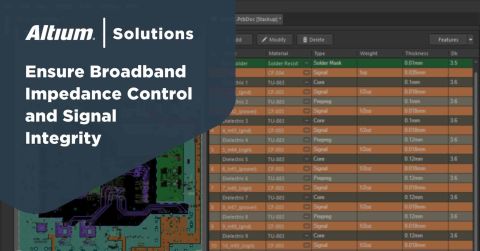
Example of board stackup parameters for a 22-layer board with FR4 materials. With an FR4 core and a prepreg set, your layer thicknesses can be larger, leading to a fairly large board thickness as well (around 3 mm in this case). Using alternative materials can result in a thinner board and possibly reduce the layer count.
Now let's try to combine this list with the ideal stackup for high speed PCBs and see if we can find a convergence.
- Signal layers need to have adjacent ground layers to provide isolation
- Power layers need an adjacent ground layer
- If the channels are very long, a low loss material might be preferable.
- Layer thicknesses may require a smaller via (blind or blind/buried) to connect the I/Os
- You need specific line widths and differential pair spacing to achieve impedance targets.
When we get to advanced boards with high layer counts, we see the convergence between HDI materials and high-speed functionality. HDI stackups that require controlled impedance and support high-speed interfaces will create challenges with line widths and spacings, to the point where non-standard processing may be necessary. The process below will go over the design challenges and should illustrate the DFM considerations needed in these products.
1. Start with board thicknesses and layers
An important point to consider for high-speed PCBs with high I/O counts is their layer thickness, which can be very thin. There is sometimes a misconception that going to very high I/O counts forces you to use a board that is thicker than the standard thickness because the layer count becomes high. This is not necessarily the case; there are materials available that can help designers stay within the standard board size target, but with low layer thicknesses.
The reason we care about layer thickness in a high-speed design is because it will determine the line width required to achieve an impedance target. As the thickness of a signal layer is reduced, the line width required for impedance-controlled signals is also reduced.
In the event that you have reached your limit on board thickness and still need to reach thinner layer thicknesses, this can push line widths below the capabilities of a standard manufacturing process or the HDI production process. Is there a material that can be used to reach a lower thickness without also reducing the line width? The answer may lie in using a low Dk material.
2. When should I use PTFE or low Dk materials?
I can't count the number of times some self-proclaimed guru has claimed that low-Dk laminates or PTFE substrates should always be used on high-speed PCBs as a general rule. It's important to remember that high-speed PCBs span a fairly wide range of possible data rates, edge speeds, bandwidths, and trace widths. There are plenty of designs that could comfortably be called "high-speed" but are not built with a low-Dk laminate. Similarly, there are plenty of high-speed designs in the HDI realm that also use a low-Dk laminate, but it's not always because they need to have low insertion loss.
Probably the most commonly cited low Dk material is ceramic-filled PTFE, which covers a huge range of possible materials . The Dk value of PTFE-based materials is modulated by the addition of ceramic fillers, so a cured PTFE substrate could have a wide range of values. For example, PTFE materials could have Dk values ranging from about 3 to about 10, all with lower losses than standard FR4 laminates. You can see a selection of PTFE materials here .
|
|
|
|
|
|
|
|
|
|
|
|
|
|
|
|
|
|
|
|
The three main reasons for using a low Dk material on advanced high-speed boards with thin signal layers are:
- Line widths can be larger than in a high Dk material for the same impedance target (See chart above)
- If the material is not reinforced, there will be no deviation due to the fiber weaving effect.
- They can be available as thin laminates, so they can be used when the number of layers is high.
These three reasons illustrate why, when you get to high layer counts, the fastest propagation delay in a low-Dk laminate is negligible, contrary to conventional wisdom. For professionals working on advanced boards, the line width issue will dominate, especially when designing high layer count boards with controlled-impedance transmission lines.

3. Balancing Loss and Dk Value
When the layer thickness is small, the line width required to achieve a particular impedance will also be small. If the line width is too small, then processing may be more challenging and costs will increase. This illustrates why point #1 above is important; a lower Dk allows for wider line widths for a given substrate thickness.
To balance low loss and high Dk, there are materials with Dk ranging from 3.5 to 4 with lower loss tangents than standard FR4; Rogers and Isola are two companies that produce these laminates, and I seem to recall another material available from ITEQ with a loss tangent ~0.01.
If low Dk is needed on a high-speed PCB at the HDI level, it will likely need to be glass reinforced. This could be reinforced with ~5 mils spread glass, but a lower thickness may need a loose weave for reinforcement. Spread glass reinforcement is intended to minimize skew buildup when the material is used for signal layers. The primary reason for this is manufacturability:
- Unreinforced PTFE laminates are very flexible, especially in thin layers, to the point that they can be difficult to handle and place in a stack.
- Due to #1, there might be some misalignment when building the layer stack in standard processing.
4. If low Dk is not always needed, why do RF designers use it?
PTFE laminates are a favorite among the RF community, and there are good reasons why we use them, but I don't think digital designers know exactly why that is. The most commonly cited reason is the low loss value of some PTFE laminates and bondplies, such as the RO3000 series materials.
One reason Dk values are carefully chosen on RF boards is to balance circuit size against loss. In fact, if you look at the list of PTFE laminates above, you'll see some high-Dk PTFE laminates with lower loss than FR4 (just calculate the imaginary part of the dielectric constant). A higher Dk value gives smaller circuits at low frequencies (e.g. sub-GHz RF), but a lower Dk can help ensure something is manufacturable at high frequencies (e.g. radar).
|
|
|
|
|
|
|
|
|
|
|
|
|
|
|
La otra razón por la que se usaría un laminado de PTFE es porque las placas RF tienden a tener canales mucho más largos en las placas digitales, por lo que los mecanismos de pérdida dominantes estarán relacionados con la propagación. Estos son la pérdida dieléctrica y la pérdida por rugosidad del cobre. Los materiales de PTFE de baja Dk de hoy en día tienen tangentes de pérdida muy bajas, lo que equivale a una baja pérdida dieléctrica. Estos laminados también pueden aceptar cobre VLP con muy baja rugosidad, por lo que también pueden ofrecer pérdidas de cobre más bajas que el cobre electrodepositado estándar.
5. Materiales de Capacitancia Embebida (ECM)
Para ayudar a la integridad de la energía, el dieléctrico que se llena entre pares de planos de potencia y tierra debe ser elegido correctamente. La sabiduría convencional sobre materiales de baja pérdida y baja Dk es incorrecta nuevamente aquí. El material utilizado entre un par de planos de potencia/tierra no debe ser un material de baja Dk. En cambio, debería tener un valor de Dk alto y pérdidas altas. Estas capas también deben ser lo más delgadas posible.
|
|
|
|
|
|
|
|
|
|
|
|
|
|
|
|
|
|
La industria ha respondido con materiales de alta Dk muy delgados que pueden incorporarse a sistemas de resina-fibra de vidrio. Estos materiales de capacitancia embebida no son necesarios para la integridad de potencia, pero ciertamente son útiles en PCBs de alta velocidad con un alto número de capas. Hay tres razones para esto:
- Alta Dk proporciona más capacitancia de plano
- Capas de ECM más delgadas tienen más capacitancia de plano
- Alta pérdida en la capa de ECM amortigua las fluctuaciones de potencia muy rápidamente
Los valores de Dk de estos materiales pueden variar de ~4 a ~10 de 100 MHz a 1 GHz. Esta es exactamente la región donde nos gustaría tener capacitancia de plano que pueda amortiguar las resonancias del plano de potencia y cualquier falta de capacitancia en el chip/en el paquete. El grosor de estos materiales será del orden de micrones. Algunas empresas que producen estos materiales incluyen a 3M y DuPont; otro material bien conocido es FaradFlex. Debido a que estos materiales también tienen pequeños grosores de capa, pueden usarse en apilamientos con un alto número de capas.
Pensamientos Finales
In the high-speed PCB stackup design process, the act of building a PCB stackup is almost the last step in the process. Instead, we care much more about layer counts and thicknesses versus component pin sizes and layout. From there, you can tackle material selection for the signal layers, and you can evaluate integrated capacitance materials for power/ground plane pairs.
If you're just designing a simpler board, such as a 4-layer board for high speed , you really only have two things to determine: the thickness of the outer layers, and the value of Dk. Together, these will determine the width of the trace you need to hit the single-ended impedance, followed by the spacing for a target differential impedance.
When you need to design your high-speed PCB stackup, use the full set of PCB design tools in Altium Designer® . The Layer Stackup Manager gives you full control over your PCB stackup, including material selection and impedance calculations. When you’re finished with your design and want to release the files to your manufacturer, the Altium 365™ platform makes it easy to collaborate and share your projects.
We’ve only scratched the surface of what’s possible with Altium Designer in Altium 365. Start your free trial of Altium Designer + Altium 365 today .

Sobre el autor / Sobre la autora
Recursos Relacionados
Related Technical Documentation
Tabla de contenido
Del diseño al lanzamiento, sin fricciones
- Mantén las revisiones vinculadas a la versión correcta
- Reduce la confusión en las transferencias y el retrabajo
- Detecta antes los riesgos de abastecimiento y liberación
- Trabaja por tu cuenta y comparte cuando sea necesario
Comenzar
Thank you, you are now subscribed to updates.


