


What is High Speed PCB Design?

At a Glance
Learn more about what is high speed board design and how to successfully design and route your high speed printed circuit board layout.


Today, most PCBs can be considered to be at risk of some type of signal integrity problem that is normally associated with high speed digital design. High speed PCB design and layout focuses on creating circuit board designs that are less susceptible to signal integrity, power integrity, and EMI/EMC problems. While no design is ever totally free of these problems, by following these high speed board design guidelines they can be reduced to the point where they are unnoticeable and do not create performance problems in the final product.
Once you’ve created your schematics and you’re ready to transition to a circuit board layout, you’ll need to leverage specific features in your PCB design tools to proper layout and routing. In your PCB design software, you’ll have an opportunity to prepare your power and ground plane arrangement in your layer stackup, calculate impedance profiles for your traces, and view PCB material options for your stackup. Most aspects of high speed design revolve around PCB stackup design and routing to ensure signal and power integrity, and the right ECAD software can help ensure success in these areas.
High Speed Digital Design Basics
So what is high speed board design? High speed design specifically refers to systems that use high speed digital signals to pass data between components. The dividing line between a high speed digital design and a simple circuit board with slower digital protocols is blurry. The general metric used to denote a particular system as “high speed” is the edge rate (or rise time) of digital signals used in the system. Most digital designs use both high speed (fast edge rate) and low speed (slow edge rate) digital protocols. In today’s era of embedded computing and IoT, most high speed circuit boards have an RF front end for wireless communication and networking.
Although all designs begin from a schematic, a major part of high speed PCB design is focused in interconnect design, PCB stackup design, and routing. If you’re successful in the first two areas, then you’ll likely be successful in the third area. Read the sections below to see how you can get started with high speed design and the important role of your PCB design software.
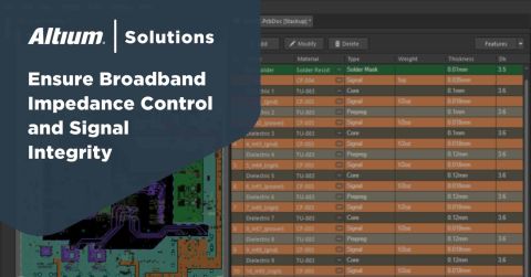
Planning Your High Speed PCB Stackup and Impedance
The PCB stackup you create for a high speed circuit board will determine the impedance, as well as ease of routing. All PCB stackups include a set of layers dedicated to high speed signal, power, and ground planes, and there are several points to consider when assigning layers in a stackup:
- Board size and net count: How large will the board be and how many nets do you need to route in the PCB layout. Physically larger boards might have enough space to allow you to route throughout the PCB layout without using more than a few signal layers.
- Routing density: In the case where net counts are high and the board size is constrained to a small region, you may not have a lot of room for routing around the surface layer. Therefore, you’ll need more internal signal layers when traces are pushed closer together. Going to a smaller board size can force higher routing density.
- Number of interfaces: Sometimes it’s a good strategy to route only one or two interfaces per layer, depending on the width of the bus (series vs. parallel) and the board size. Keeping all signals in a high speed digital interface on the same layer ensures consistent impedance and skew is seen by all signals.
- Low speed and RF signals: Will there be any low speed digital or RF signals in your digital design? If so, these may take up space on the surface layer that could be used for a high speed bus or components, and an additional internal layer might be required.
- Power integrity: One of the cornerstones of power integrity is the use of a large power plane and ground plane for each voltage level required in your large ICs. These should be placed on adjacent layers to help ensure there is high plane capacitance to support stable power with decoupling capacitors.
PCB Material Options, Layer Count, and Thickness
Before designing your PCB stackup, consider the layer count needed to accommodate all digital signals in your design. There are several ways to determine this, but these methods rely on a bit of math and some past experience in high speed board design. In addition to the points listed above for considering layer count, large high speed ICs with BGA/LGA footprints can dictate the required board size. When doing BGA fanout, you can generally fit 2 rows per signal layer, and make sure to include the power and ground plane layers in your layer count when building a stackup.

FR4-grade materials can generally be used in a high speed digital design as long as the routes between components are not too long. If routes do become too long, there will be too much loss in your high speed channel, and components on the receiver end of the channel may not be able to recover signals. The primary material property to consider when selecting materials is the loss tangent of your PCB laminates. The channel geometry will also determine losses, but generally opting for a lower loss tangent FR4 laminate is a good place to start in smaller boards.
If your routes are too long, then a more specialized material might be needed as the substrate for your high speed signals. PTFE-based laminates, spread glass laminates, or other specialized material systems are a good choice to support larger high speed digital boards, where routes are very long and low insertion loss is required. A good entry-level high-Tg set of laminate materials for small-sized high speed PCBs is 370HR. For larger boards, something like Megtron or Duroid laminates are good options. Check with your fabricator to make sure your material selection and proposed stackup are manufacturable before proceeding.
- Learn more about the factors determining transmission line losses
- Learn more about materials for RF and high speed board design
Impedance Control
Impedance is determined only after you’ve created a proposed stackup and validated this with your fabrication house. The fabricator may propose modifications to the PCB stackup, such as alternative PCB material options or layer thicknesses. Once you’ve received clearance on the stackup you’ll use and layer thicknesses are finalized, you can start calculating impedance values.
Impedance is normally calculated using a formula or a calculator with a field solver tool. The impedance you need in your design will determine the dimensions of your transmission line, and the distance to nearby power or ground plane layers. The transmission line width can be determined with some of the following tools:
- IPC-2141 and Waddell’s formulas: These formulas provide a starting point for impedance estimates, and they produce accurate results at lower frequencies.
Learn more about using trace impedance formulas. - 2D/3D field solver utilities: Field solvers are used to solve Maxwell’s equations within the transmission line geometry you define for your high speed board.
Learn more about the industry’s best field solver built into your PCB stackup calculator.
Using a layer stack manager with a field solver will give you the most accurate results while accounting for copper roughness, etching, asymmetric line arrangements, and differential pairs. Once the impedance profile for your traces is calculated, it will need to be set as a design rule in your routing tools to ensure your traces have the required impedance.

Most high speed signal protocols, such as PCIe or Ethernet, use differential pair routing, so you need to design to a specific differential impedance by calculating trace width and spacing. Field solver tools are the best utilities for calculating differential impedance in any geometry (microstrip, stripline, or coplanar). The other important result from your field solver utility is the propagation delay, which will be used during high speed routing to enforce length tuning.
- Learn more about calculating microstrip impedance
- Learn more about calculating symmetric stripline impedance
Floorplanning a High Speed PCB
There are no specific rules or standards for where components should be placed in a high speed PCB layout. Generally, it’s a good idea to place the largest central processor IC near the center of the board as it will typically need to interface with all other components on the board in some way. Smaller ICs that connect directly with the central processor can be placed around the central IC so that routing between components can be kept short and direct. Peripherals can then be placed around the board to provide the required functionality.

Once components are placed, you can set up your PCB design tools to help you start routing your design. This is a sensitive part of high speed digital circuit design as incorrect routing can ruin signal integrity. However, if earlier steps were completed properly, signal integrity is much easier to achieve. You should set your impedance profile in your PCB design rules so that any routes in the design are placed with the right width, clearance, and spacing to maintain controlled impedance during routing.
Routing, Signal Integrity, and Power Integrity
Signal integrity starts with designing to a specific impedance value in your board and maintaining that during layout and routing. Some other strategies to ensure signal integrity include:
- Aim for shorter routes between components to ensure high speed signals
- Try to minimize routing through vias, ideally only using two vias into and out of an internal layer
- Eliminate stubs on ultra-high speed lines (e.g., 10G+ Ethernet) with backdrilling
- Pay attention to the need for any termination resistors to prevent signal reflection; look at datasheets to see if on-die termination is present
- Consult with your fabricator on which materials and processes can help you avoid fiber weave effects
- Use a rough crosstalk calculation or simulation to determine appropriate spacing between nets in your circuit board layout
- Keep a list of the buses and nets that require length matching so that tuning structures can be applied to eliminate skew
These important points can be encoded as design rules for your routing tools, which will help ensure you comply with best practices on high speed design.
High Speed PCB Routing
The design rules you set in your high speed design project will ensure you meet impedance, spacing, and length targets as you route your design. In addition, important rules in differential pair routing can be enforced in your routing, specifically minimized length mismatches to prevent skew and enforced spacing between traces to ensure differential impedance targets are met. The best routing tools will allow you to encode your trace geometry limits as design rules so you can ensure performance.

One of the most important points in high speed PCB routing is placement of ground planes near your traces. The layer stack should be constructed to have ground planes in layers adjacent to impedance controlled signals so that consistent impedance is maintained and that a clear return path is defined in the PCB layout. Traces should not be routed over gaps or splits in ground planes in order to avoid an impedance discontinuity that creates an EMI problem. Ground plane placement isn’t limited to ensuring signal integrity, it also plays a role in power integrity and ensuring stable power delivery.
Power Integrity
Power integrity is a broad topic that is highly relevant in high-speed PCB design. Ensuring stable power delivery to high speed components is critical in PCB design as power integrity problems can masquerade as signal integrity problems. Power integrity focuses on low-noise power delivery to components. The PCB stackup and the layout of the PDN are the major factors that determine the level of power integrity in a digital design. If done successfully, power will be delivered to fast digital components with low noise and very weak transient oscillations on power rails. Designing a high-speed PCB with good power integrity ensures the low emissions, low noise power delivery, and elimination of some SI problems seen in high-speed interconnects.
Advanced Tools for High Speed Design and Layout
The best high speed PCB design software will bring all these capabilities together into a single application, rather than forcing you to use separate workflows to overcome different design challenges. High speed PCB layout designers must perform a lot of work on the front end to ensure signal integrity, power integrity, and electromagnetic compatibility, but the right high speed layout tools can help you implement your results as design rules to ensure the design performs as expected.
More advanced PCB design software will interface with simulation applications to help you perform industry-standard analyses. Some simulation programs are specifically geared towards evaluating signal integrity and power integrity in a new design, as well as examining EMI in a PCB layout. Simulations are very useful in high speed design as they can help users pinpoint specific SI/PI/EMI problems before a design is taken into manufacturing. Some examples include return path tracking, locating an impedance discontinuity in traces, and ideal placement of decoupling capacitors to prevent EMI.

When you need to build advanced high speed digital systems while ensuring you maintain signal integrity and power integrity, use the best set of high speed design and layout tools built on a rules-driven design engine. Whether you need to layout a dense single-board computer or a complex mixed-signal PCB, the best PCB layout tools will help you stay flexible as you create your high speed PCB layout.
Circuit designers, layout engineers, and SI/PI engineers trust the advanced design tools in Altium Develop for high speed design and layout. When a design is finished and ready to be released to manufacturing, Altium Develop makes it easy to collaborate and share your projects.

About Author
Related Resources
Related Technical Documentation
Table of Contents
- High Speed Digital Design Basics
- Planning Your High Speed PCB Stackup and Impedance
- PCB Material Options, Layer Count, and Thickness
- Impedance Control
- Floorplanning a High Speed PCB
- Routing, Signal Integrity, and Power Integrity
- High Speed PCB Routing
- Power Integrity
- Advanced Tools for High Speed Design and Layout
Design to Release, Without the Friction
- Keep reviews tied to the right version
- Reduce handoff confusion and rework
- Spot sourcing and release risk earlier
- Work solo, share when needed
Get Started
Thank you, you are now subscribed to updates.

