


PCB Signals: Key Elements of High-Speed PCB Design


Understanding the Challenge
The purpose of this article is to introduce the key elements of high-speed design and then discuss how each of those elements is tackled in Altium Designer. This article does not attempt to provide a complete discussion of high-speed design; for that, there are a number of highly experienced and scholarly designers and engineers that have written excellent reference papers and books on the subject. Refer to the References section for links to these authors, and the papers used during research for this article.
So exactly what makes a PCB design a high-speed design? Sure it’s about things happening quickly, but it’s not just about the clock rate used on the board. A design is a high-speed design when it includes devices with fast edges - devices that switch state so quickly that the transition is complete before the signal can travel along the route and reach the target pin. In this situation the signal can be reflected back to the source pin, degrading or destroying the original signal data. A signal with a fast edge can also radiate from the route and couple into adjacent routes, or radiate further and become electromagnetic interference (EMI), resulting in the product failing to meet mandatory emission standards.
When a signal has fast edges, it changes the way that the energy travels through the routing. In a circuit where edge rates change slowly, you can think of the energy flowing through the routing like water through a pipe. Yes, some energy is lost due to friction as the water is pushed through the pipe, but basically most of it arrives at the other end. For a DC or low switching frequency circuit you can work out the resistance of the route and make sure that the amount of energy lost along the way does not affect the circuit performance.
It's not so simple in a high-speed design because as well as the energy flowing as electrons through the routing copper, in a fast-switching signal, some of that energy also travels as electromagnetic energy around the routing copper. Now you are no longer designing copper pathways for electrons; you're designing a series of transmission lines embedded in a printed circuit board.
How Long is too Long?
As the switching speed of the edge increases, the energy traveling through a route behaves differently. It no longer travels like water inside a pipe. instead, most of the energy is concentrated at the very surface of the route (known as the skin effect), with a portion of the energy actually traveling as electromagnetic radiation. Not traveling through the actual conductor, this electromagnetic energy travels through the material surrounding the route. Like dragging your foot through water, when energy travels in this way the signal actually slows down. Now it is the properties of the material around the route that dictate how quickly the signal travels and how much its arrival will be delayed.
So when does this become a problem, the time it takes for the signal to propagate down the route to the target pin? Like a wave hitting a wall, when the signal arrives at the target input pin some of the energy in the signal is reflected back towards the source pin. If this reflected energy arrives back at the source pin while the original signal edge is still transitioning, the original signal will be strong enough to swamp the reflection as it completes its transition and your signal will be OK. But if the edge transition is completed before the reflected energy arrives back, like an echo in the canyon, that reflected energy will interact with the original signal and change it, perhaps so much that you cannot work out what was actually shouted into the canyon.
To summarize, when the travel time along this round-trip length is equal to or longer than the rise time of the signal, the integrity of that signal is in doubt and your design is now a high-speed design! The length of that route is referred to as the critical length - routes shorter than this should not experience signal integrity issues, whereas routes longer than this might.
To analyze your design, a common rule of thumb that is often used is the 1/3 rise time rule, which states that if the route is more than 1/3 of a rise time long, reflections can occur. For example, if the source pin has a 1 nSec rise time, then a route longer than .33 nSec - which is approximately 2 inches in FR4 - must be considered to be a transmission line and therefore a candidate for signal integrity issues.
The 1/3 Rise Time Rule:
The speed at which electrical energy can travel along a route is known as the propagation velocity and can be defined as:
Vp= C / √εR
where:
Vp = Propagation Velocity
C = Speed of Light (11.80285 in/nSec or 299.792458 mm/ns)
εR = Dielectric Constant
Assuming the Dielectric Constant εR of FR4 is 4, the Velocity of a Signal in FR4 is given as:
Vp(FR4) = (299.792458 / √4) mm/ns
=149.89 mm/ns (approx 6 inches/ns)
Applying the 1/3 Rise Time Rule of Thumb, transmission line effects will begin when:
LR ≥ (TR / 3) × (C / √εR)
where:
LR = Length of a route (in mm)
TR = Signal Rise Time (in ns).
For FR4, the route length at which transmission line effects need to be considered can be calculated as:
LR ≥ TR × 49.965 mm
If TR = 1nS
LR ≈ 50mm (2 inches)
If TR = 100pS
LR ≈ 5mm (0.2 inches)!! On a board with signals switching at these speeds, most routes will be transmission lines.
Matching the Impedances
Since it is not possible to ensure that all routes are shorter than the critical length, how do you ensure that the information encoded in your signals is received correctly, and not swamped by reflections? You do that by minimizing the amount of energy that is reflected back. Ideally, you want all of the energy that arrives at the target input pin to pass through into that component and none to be reflected back. Just how do you get that to happen?
To prevent reflections, you need to think of and design the route as if it is a transmission line. Why? Because a transmission line has the special behavior that when it is terminated by an impedance the same as its own impedance, no energy is reflected. Now you have a method of handling those routes that are longer than the critical length; route them as a transmission line. This means you route them so they have a specific impedance, then terminate them with the same impedance.
The impedance of the routing is defined by the dimensions of the routing (the width and height of the pipe), and the properties and dimensions of the surrounding materials, which will be the surrounding air or dielectric layers. To function as a transmission line, the layer that is adjacent to the signal layer must be a plane layer. By carefully arranging the layers in the layer stack and calculating the dimensions and properties, a specific impedance can be achieved for the routing. This approach to routing is referred to as controlled impedance routing, where the target impedance is kept constant, and the material dimensions and properties are selected and adjusted to achieve that.
A controlled impedance PCB cannot be achieved through routing alone though. There are two pieces to this puzzle - controlling the impedance of the routing, and matching that impedance to the pins in the net. Achieving this matching often requires the addition of termination components. Terminations can be added close to the source pin, or close to the target pin. A good approach to working out if a high-speed net needs terminating is to analyze the design with a signal integrity simulator. Unlike a circuit simulator, which models and simulates the behavior and interaction of the components, a signal integrity simulator models the behavior of the routing and its interaction with the component pins. For signal integrity simulation the components are only modeled in terms of the I/O characteristics of their pins.
The signal integrity analysis tool needs to:
- Identify nets that could have unacceptable levels of reflections (ringing)
- Predict the potential levels of signal reflection and crosstalk as waveforms
- Allow what-if analysis of potential termination components and help select suitable termination components
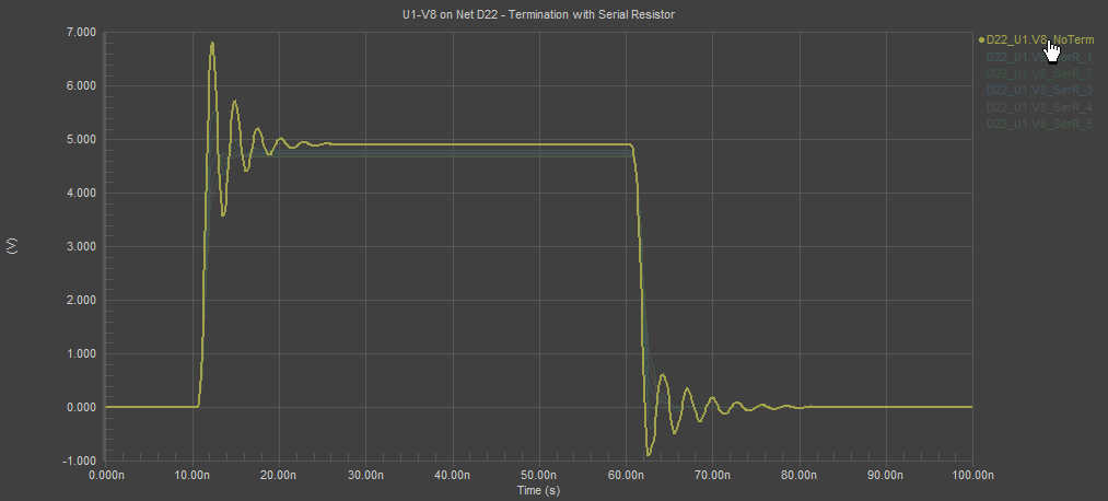

A series of overlaid waveforms that represent the behavior of a net being swept over a range of possible termination values. Left is unterminated, the right is with a theoretical 40Ω series terminator.
Where does the Return Energy Flow?
But wait, there’s more (or is that Moore?). Electrical energy only flows when there is a closed-loop, so the energy flowing out along the signal route must also have a return path. This return path is typically provided by the ground routing that has to provide a return path for all of the signals in the design. There’s an interesting phenomenon that occurs with signals with fast switching edges. The returning energy of a signal wants to flow back along the same twisting and turning path that the signal route took across the board. Why? Because this is the path of least impedance for that signal. Even though it could flow the shortest distance from the target component back to the source component, it does not.
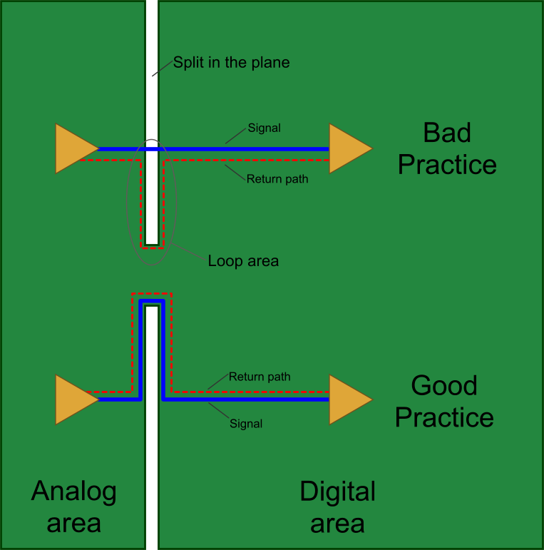
When a high-speed signal crosses a split in a plane, a loop is created, causing that signal to create EMI.
So as well as thinking about the routing path for the signal, you also have to ensure there is an unbroken path for the return current immediately under the signal route. If the return energy has to deviate from below the signal path to get around an obstacle, like a hole in the plane (a blowout), then a loop is created. The loop is the gap between the two paths as you look down into the board, and the area of this loop is proportional to the amount of energy that will now be radiated by this signal. If there is a blowout in the plane that is unavoidable, consider rerouting the signal trace to suit the return path, as reducing the loop area is generally considered more important than minimizing the route length.
An important point to keep in mind is that the return path is through the closest power plane, which might not be a ground plane. If the return path is through a power plane instead of a ground plane, the return energy will ultimately get to ground through the decoupling capacitors that are closest to the source and target pins. If you are relying on a power plane to provide the return path, carefully consider the location of the decoupling capacitors near these pins to minimize the size of any loop created.
Differential Pairs
Modern signaling technologies, such as differential pairs, help reduce the need for a high-quality return plane by routing the signal path and the return path together as a pair, ensuring that they are closely coupled in both separation and overall length. As well as the strong coupling and the reduced reliance on a high-quality reference ground, differential pairs offer another big advantage - excellent immunity to noise.
The electromagnetic energy that is traveling around the route as part of each signal does not all couple into the target input pin; some of it escapes and interferes with adjacent signals. This escaped energy becomes what is called electromagnetic interference (EMI), and when it couples into a neighboring signal, it creates what is called crosstalk. Differential pairs are good at coping with crosstalk because the radiated energy couples into both the outgoing signal and the return signal, creating what is called common-mode noise (the noise is common to both signal paths). If there was only a single signal, this crosstalk would add to that signal and distort it. But the differential pair input pins are designed to look at the difference between the pins in the pair, and so are able to reject the common-mode noise.
These two qualities - the ability to closely match the lengths of the signal and its return path, and the ability to withstand the effects of crosstalk - make differential pairs the preferred solution for high-speed signaling, which can support data rates beyond 10 Gb/s on a PCB.
Differential pairs provide strong immunity to noise and reduce the reliance on a high-quality return path via a plane. This reduced reliance on a ground plane is directly related to the degree that the pair lengths are matched and remain consistently coupled - as the length matching or the coupling declines, the reliance of the signals on the plane increases. Most experts agree that matching the length is the critical requirement for differential pairs.
What about Vias?
If carefully controlling the impedance and insuring there is a high-quality return path are the first two edges of the high-speed design triangle, vias are the third edge of that triangle. At low frequencies, a via has little impact on the signal quality and can be used without consideration of its impact on circuit performance. However, if your design is functioning as a high-speed design, the vias can impact on the circuit performance and the signal quality.
Vias appear as both capacitive and inductive discontinuities, so their presence affects the impedance of the signal route. As well as affecting the impedance, unused via barrel length presents as a stub which can create reflections. Quantitative studies have shown that their impact can be reduced by addressing each of the following areas:
- Reducing the size of the annular ring where the signal route connects to the via.
- Removing unused annular rings on layers to which the via is not connected.
- Increasing the clearance from the via barrel to adjacent plane layers.
- Placing stitching vias adjacent to signal vias to provide a path for the signal return current to be able to switch plane layers.
- Careful placement of decoupling capacitors adjacent to the via when a different voltage plane will be used to carry the signal return.
- Removal of via stubs (the extra, unused via length that projects beyond the layer that the signal route uses to access the via). This is done through:
- via design and careful layer assignments to suit the fabrication process, and
- controlled depth drilling (back drilling) to remove the unused section of the via barrel.
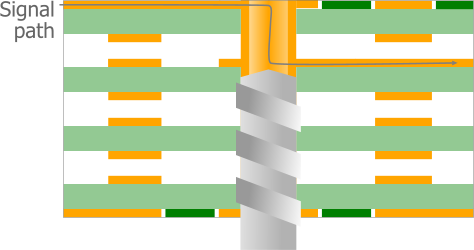
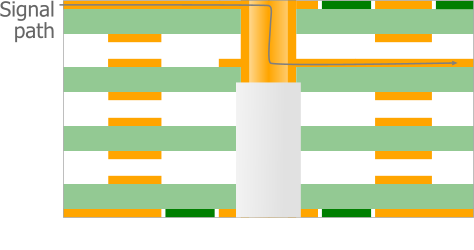
Using a controlled depth drilling process, often referred to as back drilling, unused via barrels can be removed.
Another approach to minimize the impact of vias in a high-speed design is to use microvias. A microvia is a small via. IPC standards (IPC/JPCA-2315 and IPC-2226) define microvias as blind or buried vias with a diameter equal to or less than 6 mils (0.15 mm). A 6 mil diameter is at the limit for mechanical drilling so microvias are typically laser-drilled. There are also hybrid laser modified + controlled depth mechanical hole drilling techniques used, as outlined in this paper, which offers advantages in fabrication.
Microvias offer a number of advantages:
- Reduced parasitics (in the order of one-tenth of a drilled thruhole via), resulting in lower inductance.
- Smaller geometries, which result in a smaller annular ring.
- Reduced size of blowout on plane layers that they pass through.
- Removal or reduction of stub length. Because they are constructed as part of the layer stacking process during fabrication, they can connect between specific start and end layers. While they cannot span any pair of layers, careful selection of the signal layers used for high-speed signals can ensure that those layers have access to a microvia start/stop layer.
Suitable via design is an important ingredient in the high-speed board design process. The possible layer-to-layer via connection possibilities are dictated by the board fabrication process, making it essential to choose the fabrication and drilling process at the same time as the via style and the layer stackup is being defined.
Crosstalk
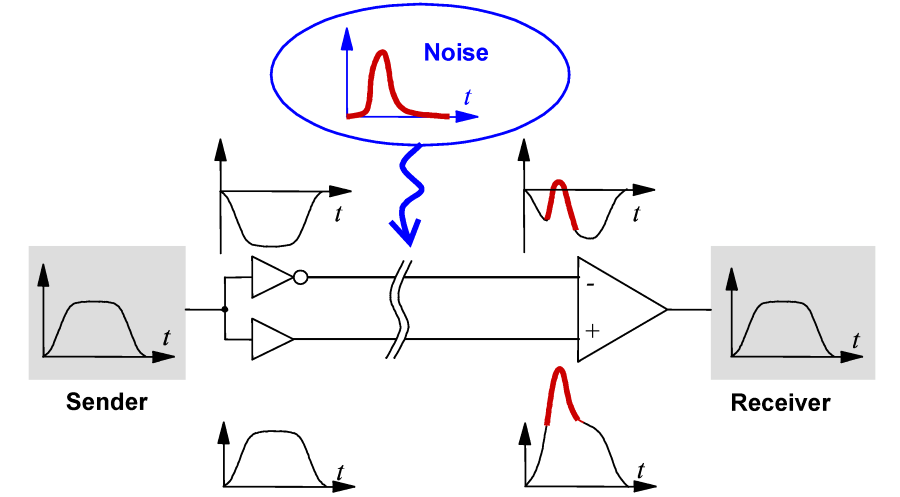
Because some of the energy in a high-speed signal travels through the material that surrounds the route, it is inevitable that some of that energy will couple into adjacent routes. Referred to as crosstalk, this energy will degrade the quality of that signal. In signal integrity language, the signal that is radiating the energy is referred to as the aggressor net, and the signal that is receiving the crosstalk energy is referred to as the victim net. So how do you reduce the amount of energy that escapes from the aggressor, and how do you reduce how much of that energy is coupled into the victim? The basic approach is to reduce the amount of energy escaping from the aggressor route through impedance matching and correct design of the signal return path, and to keep potential victim nets away from aggressors.
Clock signals and other periodic signals are the prime sources of crosstalk in a design. An often-used rule of thumb is to ensure that potential aggressors, such as clocks, are separated from potential victims by three times the width of the routing (measured center to center). This is known as the 3-W rule. Or in edge-to-edge terms, the separation must be no less than twice the routing width. This is a large clearance, so you will need to be selective about the nets to which it is applied. High-threat aggressors, such as clocks, are one group. The other main group to consider is the more sensitive potential victims, such as differential pairs; this group also benefits from a pair-to-other-signal separation of 3-W.
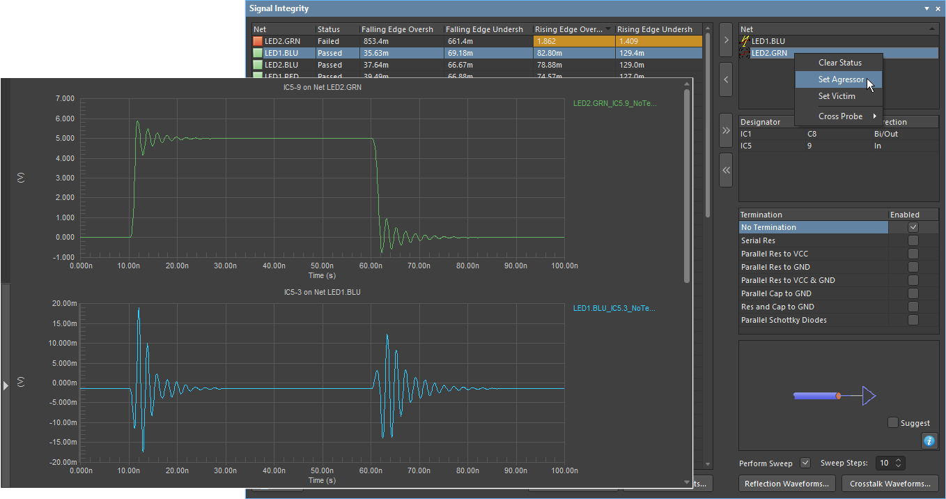
Predicted ringing on an unterminated aggressor route (green waveform), and the resultant crosstalk in the adjacent victim route (blue waveform). Note that each graph has a different voltage scale.
Dancing in Time
Last but not least, there is the time it takes for the signal to arrive at its destination input pin. Generally, a signal does not exist in isolation. It is working in harmony with a multitude of other signals. A simple example would be the 8 bits in a byte of data. Not only must the entire byte arrive within the time allowed, the bits within the byte must all arrive together too. The time it takes for a signal to travel from output to input is referred to as the flight time, and any difference between the arrival times of the bits is referred to as the signal skew.
The key factors that influence both the flight time and the skew are:
- The length of the signal routes, i.e. how far the signals have to travel.
- The materials that the signals are traveling through; this affects how fast the signals travel.
Managing these requires consideration of:
- Component placement - good component placement is a key element of a successful high-speed design. Use the Manhattan length to guide the initial placement of different components that need similar route lengths, for example, DDR3 memory devices configured in a T-branch topology.
- Material selection - the material from which the PCB is fabricated is a critical factor in a high-speed design. FR4 has served the PCB industry well for decades, but its use becomes a limiting factor in high-speed designs since the inconsistent dielectric constant of FR4 creates skew. Material is discussed more in the following section.
- Overall route length - as well as influencing the flight time, overall lengths are also important when routing sets of related nets. For example, DDR timing requirements specify that the clock route is longer than the address and control routes. These requirements are managed by Length design rules.
- Matched route lengths - skew is managed by matching route lengths. It is the longest route in a set of signals that determines the route length for each net in that set. Lengths are matched by defining Matched Length design rules, then lengthening each shorter route to match the specified length.

Differential pairs - lengths are matched within the pairs, and also between the pairs (image courtesy FEDEVEL Open Source, www.fedevel.com).
The Board
All of this happens on the printed circuit board. Since they were first created in the 1940s, the humble PCB has undergone tremendous levels of refinement in fabrication technology and materials. This has lead to enormous reductions in the size of the features, including the routing and vias. Tracks are no longer fabricated at 20 mils wide. Now they can be as small as 2 mils wide; and a small via is no longer 30/18 mil (land/hole) - it is 12/6 mil. A new name was created to describe designs using features this small - High-Density Interconnect (HDI) techniques. While it costs more to create the smaller features used on HDI boards, their smaller size means the finished design can use fewer layers, have shorter routes, and improved signal integrity, which can ultimately result in a board that might not cost any more to make (but can be much harder to test and repair).
The Materials
A large part of the challenge with a high-speed design is managing the medium that the signals travel through. Traditional FR4 has provided a cheap and effective board substrate material for decades, but the non-homogenous structure of fiberglass weave embedded in resin becomes a limiting factor for high-speed designs. The resin has a different dielectric constant (≈3) from the fiberglass weave (≈6), and since the fiberglass is a woven structure with gaps in the weave, the signal sees a changing dielectric constant as it travels across the board. Because of this, there is a range of FR4 materials available. Better materials have a tighter weave structure that gives a more consistent dielectric constant. The dielectric constant of FR4 also changes with temperature by as much as ± 20%.
There are superior materials available for PCB fabrication, such as Teflon or ceramic, but these come at a price. The material that the board is fabricated from must be considered and chosen early in the PCB design process in consultation with the fabricator. To help balance material selection against material cost, many PCB fabricators allow a mix of materials so that the expensive materials are only used for the layers that carry the high-speed signals.
The Layers
Like many aspects of printed circuit board design, working out the best number of layers is as much art as it is math. Fanout and escape routing of dense BGAs will strongly influence the number of routing layers. Performing a test fanout and escape route to check the densest BGA in the design can help verify there are enough signal layers. Another approach, recommended by Barry Olney of In-Circuit Design, is to run a test autoroute on the board. He suggests that if it completes at least 85% of the routes, the board should be hand-routable using the current layer stackup.
Adding and assigning layers is done in pairs. Generally, you will either have a pair of plane layers for each pair of signal layers, or a pair of plane layers for every two pairs of signal layers. So a four-layer board will be two plane and two signal; a six layer board will be two plane and four signal, an eight-layer board will be four plane and four signal, and a ten layer board will be four plane and six signal layers. Note that this is only a guideline; the overriding objective is to ensure that every high-speed signal layer is adjacent to a plane layer.
Not all signals are high-speed signals, and not all layers can be configured as high-speed routing layers, so the standard practice is to assign and route the high-speed signals on specific layer pairs. Each signal layer pair should have one layer in the pair assigned for vertical routing and the other assigned for horizontal routing, and these should be followed as best as possible to reduce crosstalk between the adjacent layers. The high-speed pair can be positioned on either side of a plane layer or between two plane layers.
The thickness of the dielectric between the high-speed signal layers and the reference plane layer will be set to suit the required characteristic impedance; typically this will be less than 10 mils (0.25 mm). To achieve the overall board thickness required for mechanical reasons, adjust the thickness of a dielectric layer(s) that is not adjacent to a high-speed signal layer, for example, the center core layer.
The HDI Handbook includes a packaging technology map, which can be used to indicate if a design can be implemented using traditional mechanical drilling, or if it is likely to need to use a High-Density Interconnect (HDI) structure. IPC standards IPC/JPCA-2315 and IPC-2226 include formulae that can be used to calculate component and wiring densities, providing you with valuable information to use when discussing the number of layers and the stackup options with your fabricator.
Possible Layer Stackups
The table below shows a number of possible layer stackups and layer assignments. The arrangement of high-speed pairs and general purpose pairs can be changed, for example, if your six-layer/thruhole-only design can have the high-speed signals routed on the top layer, this is a good option if it means the high-speed signals do not need to use vias. Keep each high-speed layer adjacent to a plane layer, and the surrounding dielectric thicknesses the same for the high-speed layers.
| 4-LAYER | 6-LAYER | 8-LAYER | 10-LAYER | 12-LAYER |
|---|---|---|---|---|
| Signal HS-H | ||||
| Signal HS-H | GND | |||
| Signal HS-H | GND | Signal HS-V | ||
| Signal H | GND | Signal HS-V | Signal H | |
| Signal V | GND | Signal HS-V | Signal H | GND |
| GND | Signal HS-V | GND | GND | Signal V |
| POWER | Signal HS-H | POWER | POWER | Signal H |
| Signal H | POWER | Signal H | Signal V | POWER |
| Signal V | GND | Signal HS-H | Signal V | |
| Signal V | GND | Signal HS-H | ||
| Signal HS-V | GND | |||
| Signal HS-V |
Suggested layer stackups for 4, 6, 8, 10, and 12 layer boards.
Define the layer stackup early and pay close attention to the start/stop layers available for vias.
Now that you understand the challenges of High-Speed PCB design, learn more:
- Altium Designer features for High-Speed Design
- Documentation on tackling these challenges directly in Altium Designer
Related Resources
Related Technical Documentation
Table of Contents
Design to Release, Without the Friction
- Keep reviews tied to the right version
- Reduce handoff confusion and rework
- Spot sourcing and release risk earlier
- Work solo, share when needed
Get Started
Thank you, you are now subscribed to updates.