


High-Speed PCB Design Guidelines and Techniques in Altium Designer


High-speed PCB layout and routing can be complex and requires many diverse considerations. Important high-speed layout techniques and routing guidelines for your design span everything from trace widths on transmission lines to ground pour clearances, return path tracking, defined characteristic impedance, and much more. Simple design software packages simply can’t handle all of these constraints at once, leaving the circuit board designer to manually check every interconnect and spend hours reworking the layout when errors are identified.
Altium Designer is the only design application that was built to handle any electronic product. Design teams can quickly and easily implement the best high speed PCB design guidelines to ensure signal integrity with an advanced toolset in a single application. PCB designers know that creating a high-speed PCB layout requires many calculations, measurements, and conformance to design rules, and Altium Designer helps automate many of these important tasks. If you want to streamline your design process without sacrificing signal integrity, be sure to implement these high speed PCB design techniques and high speed board design guidelines in your next circuit board.
ALTIUM DESIGNER®
The industry’s best electronics design and simulation application for professional designers and PCB manufacturers.
Today’s modern electronics run at faster speeds, are placed with higher density and require more accurate routing than ever before. The expectation is that high-speed designs will only have increased capabilities in the future, and designers need to implement the best high-speed PCB design guidelines and routing practices to ensure their designs operate properly. Important aspects of a design like impedance control, return path planning, and high-frequency EMI are just the start in high-speed PCB layout.
While there are many requirements to satisfy in any high-speed circuit board layout, the right design software can help by allowing you to specify these requirements as design rules. These rules are then enforced as you place your components and route your high-speed transmission lines. Altium Designer is the ideal PCB design software package for ensuring your high-speed circuit board operates as required and complies with industry standards.
What is High-Speed PCB Layout and Design?
All high-speed PCBs have signals with fast edge rates, meaning the power spectral densities of various signals stretch into the high GHz range. These components on high-speed PCBs switch quickly and can generate significant EMI if not routed properly. As such, layout, routing, return path planning, characteristic impedance calculations, and many other factors determine the stability and integrity of these designs.
Some of the important high-speed PCB design guidelines in layout and routing are listed below. These guidelines are intended to help ensure signal integrity during layout and routing, as well as to help prevent EMI problems like crosstalk, radiation, and impedance discontinuities:
- Ground planes, power planes, and stack-up: Make sure the PCB stack-up has uniform ground below high-speed transmission lines and does not route over gaps in ground/power planes.
- Characteristic impedance: A specific trace width should be enforced in transmission lines to ensure characteristic impedance and input impedance have specific values on high-speed interconnects.
- Transmission line spacing: Enforce sufficient spacing between traces on the PCB to prevent significant crosstalk and ensure that signals will not exceed noise margins at the receiver.
- Power integrity: Place power and ground planes next to each other, specifically the portion of the PDN that will supply high-speed components with power to prevent excessive ringing.
- Bus and differential pair routing: Enforce timing matching on parallel buses and on differential pairs to ensure minimal skew between important signals.
- Component placement: Make sure to place critical high-speed components in the PCB layout in such a way that all critical signals are routable with minimal layer transitions.
This list of general guidelines will help ensure your design does not fall prey to signal integrity problems that are common in high-speed PCB layouts. With the best PCB design software, you can program these requirements as design rules to ensure a complex layout maintains signal integrity.
Quickly Check Your High-Speed PCB Layout Techniques Against Design Rules
Your design rules shouldn’t constrain your creativity, but rather they will help ensure your design functions as required once your layout is complete. All of Altium Designer’s routing and layout tools are built on top of a unified rules-driven design engine to ensure route-ability and compatibility with the above list of guidelines.
- Parallel buses and differential pairs require precise length/timing matching to prevent skew. You can enforce these conditions with length-tuning tools in your PCB routing features.
Learn more about delay tuning to ensure timing skew is eliminated in differential pairs.
- Don’t allow your board to fail due to common signal distortion problems. You can solve these during routing with the best PCB design tools.
Learn more about signal distortion sources with high-speed PCB design guidelines.
- You can ensure your routing meets basic design rules, maintains impedance, and satisfies skew requirements with the best auto-interactive routing features in Altium Designer.
Learn more about auto-interactive routing for high-speed PCB design.

This simple PCB requires impedance-controlled routing for high-speed signals to ensure signal integrity.
A Powerful High-Speed PCB Routing Engine
Once your components are placed in your layout, they should be carefully adjusted to ensure easy routing for low-speed, high-speed, and DC signals. Routing can be difficult in very dense designs due to the large number of components and nets, especially for high pin count BGAs. Keeping routes short between components, decoupling circuit layouts, and power supply circuits ensures losses remain low, but it takes a set of routing features that enforce design rules and impedance control in your high-speed PCB layout.
Use a Rules-Driven PCB Routing Engine for High-Speed PCB Design
The rules-driven routing engine in Altium Designer helps you comply with basic routing guidelines by enforcing your clearance constraints, routing length limit constraints, and trace impedance constraints as you work. With other PCB design software, you need to manually run DRCs once the layout is finished, leaving open the possibility of design errors and rework. Altium Designer helps you catch errors and correct them early while you create your PCB layout, which helps ensure you comply with basic high-speed PCB layout techniques.
In addition, Altium Designer’s auto-interactive routing utilities let you implement any routing topology throughout your high-speed PCB layout. If you’ve applied your clearance rules and enforced characteristic impedance control in your PCB layout, your auto-interactive routing tools will help automate routing while ensuring your layout conforms to these important design rules. These tools help ensure you won’t have major problems with EMI, skew, impedance discontinuity, and other sources of signal distortion.
- PCB routing constraints must be programmed into your design rules so that you don’t fall victim to common radiated EMI sources.
Learn more about EMI sources in high-speed and high-frequency PCBs.
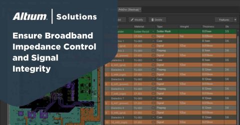
- You can easily ensure characteristic impedance control in Altium Designer’s layer stack manager. This tool allows you to create impedance profiles that are set as design rules to enforce a required trace width.
Learn more about impedance profiles for accurate routing in Altium Designer’s stack-up tools.
- If you can keep your trace lengths short enough, you can prevent skew accumulation due to fiber weave effects. Altium Designer’s rules-driven layout engine will help you set length and timing limits in your differential pairs.
Learn more about fiber weave effects and skew in high-speed routing.

Only Altium Designer gives you a complete set of design and layout tools for advanced high-speed PCBs.
High-Speed PCB Design Techniques Help You Route Accurately
As the industry’s premier circuit board design software package, Altium Designer implements an intuitive design interface that is built entirely on a rules-driven design engine. For high-speed PCB layout, you can easily define all of the above guidelines as design rules for layout and routing, which will help ensure your design will comply with basic performance metrics and will be manufacturable. Most importantly, high-speed signal integrity metrics will be checked as you route your board, and mistakes will be flagged during layout. You can spot errors early and solve them before creating your manufacturing deliverables.
With the Altium 365 platform, every Altium Designer user can share their design data alongside their fabrication files, assembly files, and test documentation. This even enables unique test methods and strategies like hardware-in-the-loop testing before and after performing PCB aging tests. Only Altium 365 and Altium Designer create a single ecosystem where designers, manufacturers, and test engineers can work together to solve complex printed circuit board design challenges.
Route Quickly and Accurately With Altium’s Rules-Driven PCB Design Software
The power of Altium Designer comes from its rules-driven PCB design engine, where all of your important design, layout, routing, simulation, and manufacturing tools come together to keep you productive. All of the PCB design features in Altium Designer were built to work together in a single, unified design interface on top of a complete set of standard and specialized high-speed PCB layout techniques. The underlying rules-driven design engine allows all your design and high speed routing techniques to share data and work together seamlessly while satisfying important design constraints.
Altium Designer also helps guide you through the entire PCB design process to ensure your board is manufacturable. Once you’ve finished your high-speed PCB layout, you can instantly generate your fabrication and assembly files thanks to an automated documentation and file creation process. You can also customize your documentation using free application extensions and additional features, such as drawing creation in Draftsman and cleaning your BOM with ActiveBOM. No other PCB design application helps you stay this productive and build advanced electronics.
- Take advantage of the powerful design rules engine in Altium Designer, the only application that helps you implement the best high-speed PCB layout techniques in a rules-driven design and layout environment.
Learn more about Altium Designer’s complete circuit board toolset.
- Altium Designer’s routing engine was built to handle high-speed PCB routing requirements and interfaces directly with your design rules engine.
See Altium Designer’s advanced PCB routing engine in action.
- Don’t use 3rd party services to share your high-speed PCB project files, use the secure cloud platform in Altium 365. You can quickly share your project data and collaborate with other designers with the Altium 365 platform.

Altium Designer includes everything needed to design high-speed PCBs and implement the best layout techniques.
The rules-driven design interface in Altium Designer is key to ensuring your design will be manufacturable at scale while also following basic PCB design and high speed layout guidelines. The rules-driven design interface in Altium Designer ensures you can implement the best high speed PCB design layout techniques to maintain signal integrity and to ensure your design intent will be satisfied. Keep your designs running smoothly with Altium Designer and Altium 365.
Altium Designer on Altium 365 delivers an unprecedented amount of integration to the electronics industry until now relegated to the world of software development, allowing designers to work from home and reach unprecedented levels of efficiency. There are multiple tutorials ripe with additional high-speed PCB design guidelines for you to take advantage of as well.
We have only scratched the surface of what is possible to do with Altium Designer on Altium 365. You can check the product page for a more in-depth feature description or one of the On-Demand Webinars.

About Author
Related Resources
Related Technical Documentation
Table of Contents
Design to Release, Without the Friction
- Keep reviews tied to the right version
- Reduce handoff confusion and rework
- Spot sourcing and release risk earlier
- Work solo, share when needed
Get Started
Thank you, you are now subscribed to updates.