Connect and Conquer: Multiboard Design Adaptation in PCB Design Software
Years ago I designed boards at a service bureau where there were several different customers and the boards that I worked on were unique in size and function. And in all of those designs, none of them were ever from the same system. Not only was it more to spread the design work around back then, but the only way to do system design was to create the boards individually and then test the prototypes together.
With faster times to market and shrinking design budgets, using PCB prototype builds to test and verify system design is getting more difficult. Fortunately, PCB design tools today can offer a lot of help. With the ability to bring multiple PCB designs into the same design session, you can check for connectivity between the printed circuit board as well as check how they will mechanically fit together. Using Altium Designer® lets me show you the basics of how this works.
Preparing for a Multi-PCB Assembly
Altium gives you the ability to verify the connectivity and fit of multiple system PCB layouts with its multi-circuit board functionality. To demonstrate how this works, I am going to use a very simple example design with a simple 2-pin connector on it. My base design is named “Example_Design”, and I also made a copy of it where I changed the reference designators and some of the physical placement called “Example_Design2.”
Adding the multi-board connector property to a connector component in Altium Designer
The first thing that you, as a PCB designer, have to do is to make sure that your single circuit board schematics are prepared for the multi-board schematic. To do this you need to add an Altium multi board connector parameter to the connector components in your single-board schematics in order to identify them as multi-board connectors. As you can see in the picture above, I opened up the properties of the connector components and added a “System” parameter with the value of “Connector”.
Creating the Schematic in PCB Design Software for Multi Board
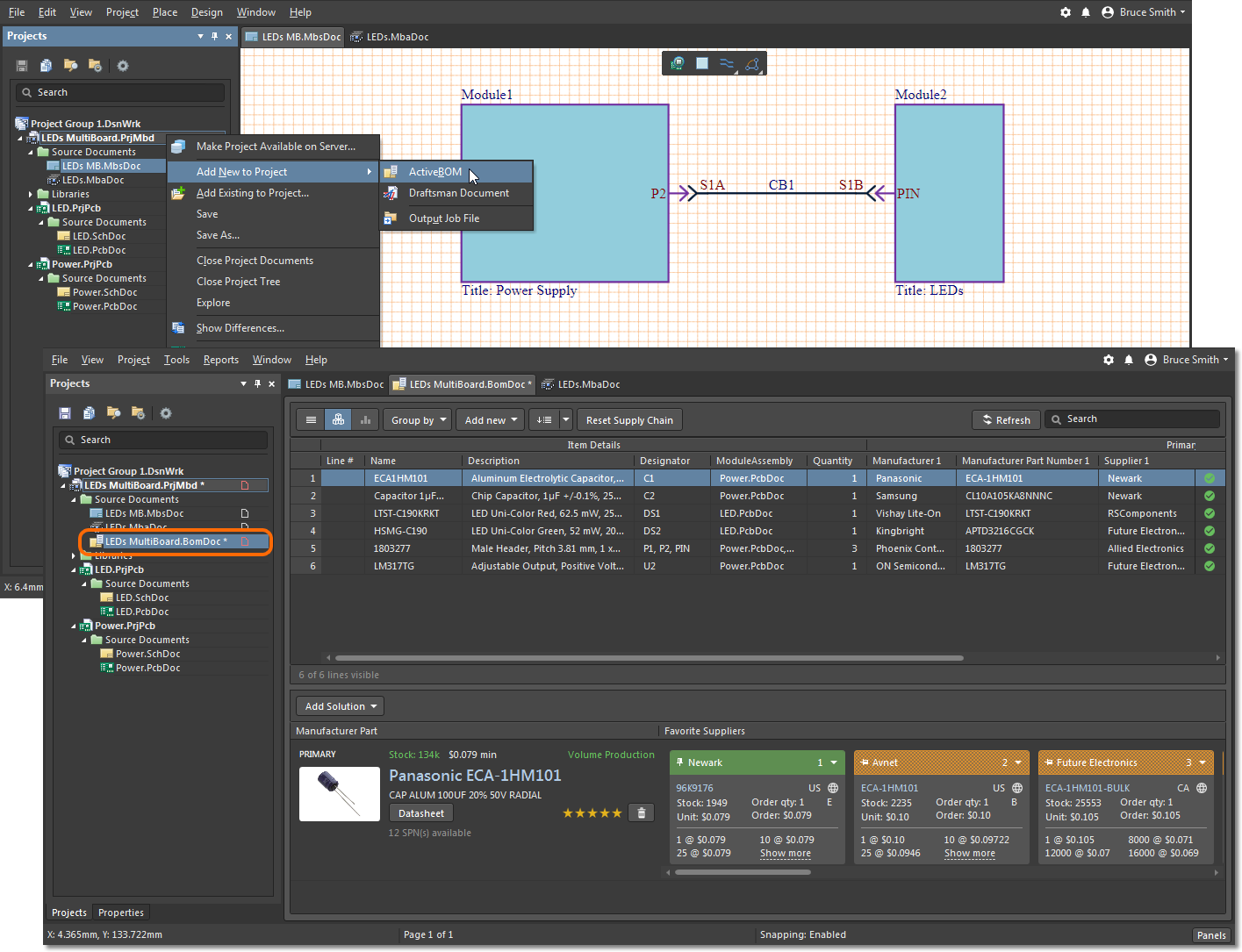
To work with multiple PCB designs in a single session in Altium Designer you must first create a multi-board project. You can create the project in an existing project folder, or as in this case, I created a new folder for my multi-board project. To create the project I used the “File > New > Project > Multi-board Design Project” menu command and saved it in my new folder with the name; “Multiboard_Example.”
Next, I right-clicked on the Multiboard_Example project and added a new multi-board schematic to the project as shown in the picture below. As with the project I also saved this with the name “Multiboard_Example”. At this point, I now had an empty multi-board schematic in my design session.
Adding the schematic to the multi-board design project
Now it was time to start adding the circuitry from the two different designs into my multi-board schematic. To do this I added a module using the “Insert Module” icon in the taskbar as shown in the picture below. Once I had added this first module, I copied it to create another module just to the right of the first one.
Inserting some individual designs as modules in the multi-board schematic
Note that the freshly created modules above have simple numbers for designators and they are both untitled. To fill in this information I first selected the module on the left and opened up its properties. I gave it the designator of “PCB_1” and the Title of “Example_Design.” You can see in the picture below how the module itself updated once the properties were entered on the left.
Changing the module properties in Altium Designer’s multi-board schematic
You also will need to identify the source of the individual circuit board laptop database which I have done in the picture above. In the “Source” section of the properties, I clicked on the triple dots next to the “Source” item which opened up a navigator. This allowed me to find my single board “Example_Design” project and select it. Immediately below that the path to the “Assembly/Board” automatically fills in from the single board schematic that you had selected.
Once I finished the first module, I repeated this same process with the second module. I used “PCB_2” and “Example_Design2” for the designator and the title, and I navigated to the Example_Design2” project for the source.
Now that my modules had the desired properties that identified what they were and where their source data came from, it was time to import the source design data. To do this I first selected the module on the left (PCB_1) to activate it and then went to the “Design > Import From Selected Child Projects” pulldown command. This takes a bit as Altium Designer is pulling the design data from the single circuit board project, and when it is ready it will pop open the “Engineering Change Order” dialog box that you see in the picture below.
Importing the design data from the child project into the multi-board board schematic
You will need to first validate the changes in the dialog box by clicking on the lower left button, and then execute the changes by clicking the button next to it. You can see in the picture above that I have already done this. The result is that it has gone into that individual board schematic, found the 2-pin connector that we first assigned the connector property to, and placed a module entry (P1) for that connector on the module in my multi-board schematic.
Once you’ve completed the same process for the other module, you are ready to create a logical connection. Before creating the logical connection, it’s a good design practice to clean up the modules to make them more usable. You can see that I have repositioned the module entries for both P1 and P101 to make them easier to work with. Just grab them with the mouse and move them to your desired location.
To add a logical connection between these module entries, use the “Add Wire” icon in the taskbar. By holding your mouse button down on the icon you can see that you have the option of adding a wire, a direct connection, a cable, or a harness. I chose a wire and routed the connection between the two module entries as shown below.
Adding the logical connection between the individual designs in the multi-board schematic
Once the logical connection is routed you can move the text around as desired. You can also select the logical connection and see the individually printed circuit board connections in the properties panel as shown above. By selecting those individual connections in the properties panel you can change the pin assignments or add and delete pin assignments as needed.
Placing and Orienting the 3D PCB Layout in Your Design Session
Now that connectivity has been set up in the multi-PCB schematic, it’s time to create the physical PCB layout in the multi-board assembly. To do this I once again right clicked on the Multiboard_Example project and added a new multi-board assembly. As with the project and the schematic I also saved this with the name “Multiboard_Example”.
The next step will be to associate the design data in the project with the new multi-PCB assembly. To do this I used the “Design > Import Changes From (Project Name)” command. This pops up another “Engineering Change Order” dialog box, and once I had validated and executed the changes in the dialog box, my two individual layouts were displayed as shown below.
Importing the individual physical design data for Altium Designer's multi-board project
You can see in the picture above that both designs are shown together. At this point, I clicked on the board outline to select one of the designs which turned green in color. You can see the overlapping and part of the board outline of the second design protruding on the right side. Now you need to separate the two for better viewing.
I had already selected the larger board as shown by its green color in the above picture. Once activated like this you can now grab it with the mouse and move it to one side so that you can see both designs. You can see in the lower left corner of the activated board some colored arrows and arcs. By grabbing and dragging these “Workspace Gizmos” you can control the orientation of the selected board.
I manipulated both boards so that they were angled into each other. They are also positioned so that their connectors are facing each other. You can see the final position of the boards in the picture below.
Viewing both boards in 3D using Altium Designer’s multi-board project
There are many other things that you can do with the multi-board assembly functionality in Altium Designer. You can make connectivity changes and update those changes. You can also import 3D mechanical data so that you can see your boards as well as mechanical features such as cases and enclosures all within the multi-board assembly. We’ve only scratched the surface here to give you this basic overview of multi-circuit board design.
Altium Designer is one of the best PCB design software tools that you can use today because of abilities like what I have just described. With multi-board assembly as part of your standard design toolset, Altium Designer will help you to save time and money by reducing the number of PCB prototypes that you have to build. For system design and other design challenges, Altium Designer is the tool that you need.
Would you like to find out more about how Altium Designer can help save you time and money with its multi-board system design capabilities? Talk to an expert at Altium Designer.


