Skip to main content
Mobile menu
Discover
Develop
Agile
Resources & Support
Free Altium 365 Tools
Gerber Compare
Online PCB Viewer
Resources & Support
Learning Hub
Support Center
Documentation
Webinars
Altium Community
Forum
Bug Crunch
Ideas
Education
Student Lab
Educator Center
Altium Education Curriculum
Search Open
Search
Search Close
Sign In
Main menu
Home
PCB Design
Collaboration
Component Creation
Data Management
Design Outputs
ECAD/MCAD
HDI Design
High Speed Design
Multi-Board
PCB Layout
PCB Routing
PCB Supply Chain
Power Integrity
RF Design
Rigid Flex
Schematic Capture
Signal Integrity
Simulation
Software
Develop
Discover
Agile
Altium 365
Altium Designer
Education
Programs
Altium Academy
Engineering News
Guide Books
Newsletters
Podcasts
Projects
Training Courses
Webinars
Whitepapers
Real-Prototyping World
There’s something to be said about the difference between designing your system on an evaluation board compared to designing it using the board on which your system is actually going to ship. One of the problems with using an evaluation board is that it’s a really nice environment to work in. Too nice, in some respects. The processor company wants you to have a positive experience with their chip so the eval board has all the bells and whistles
Read Article
Riding Technology Waves
There’s tremendous value in being able to utilize the latest and greatest technology on the market. Of course, the leading edge is sharp and there are ways you can cut yourself if you aren’t careful. In general, though, having the flexibility to choose where you ride technology waves enables you to better balance the overall performance, cost, and power efficiency as you design systems. I remember an industrial embedded system I was optimizing
Read Article
Quit Bouncing Around
Bounce on a single-pole, double-throw (SPDT) switch with normally closed (NC) contact opening and normally open (NO) contact closing (Image source: David Ashton) In an earlier column -- Say "Hello" to the LogiSwitch Workbench -- I introduced a rather clever shield for the Arduino Uno. This little scamp allows you to break out all of the Arduino's analog and digital input/output (I/O) pins, along with the 5V, 3V3, and GND pins, to three full-size
Read Article
All Hail the Evo Compute Module
The Evo Compute Module (small board) mounted on an EvoTray (larger board) (Image source: Alorium Technology) I was just chatting with my chum Jason Pecor at Alorium Technology. We bounced around from topic to topic with the agility of much younger men. At some stage in our conversation, Jason mentioned a forthcoming product called the Evo Compute Module, which really grabbed my attention. I'll tell you all I know in a minute (it won’t take long)
Read Article
Accelerating Board Bring Up
There’s that moment when you power up the first production board for a new design. It doesn’t matter how perfectly the prototypes operated. The question, “Is it going to work?”, still hangs in the air. At its best, this process is exciting. At its worst, you find yourself with an intermittent but persistent problem that means you need to spend more time and money. Today, there are a great variety of off-the-shelf boards available to jumpstart
Read Article
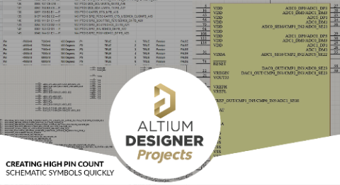
Creating High Pin Count Schematic Symbols Quickly
Making schematic symbols is quick and painless when you use regular expressions and leverage Altium Designer’s expansive toolkit.
Read Article
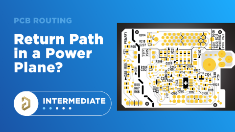
Power Plane and Ground Planes: Should You Use Your PCB Power Plane as a Return Path?
Power planes (sometimes called a power layer) and ground planes are important for more than just distribution of supplying power. When defining reference planes, both with impedance controlled routing and in managing return paths, your stackup might force return currents to pass into a PCB power plane before being coupled back to a ground layer. Even though you define a GND reference layer as a the basis for your impedance-controlled trace width
Read Article
Lies Your Fabricator May Have Told You
In some of our previous articles, we have talked about the various things that go wrong when a board design is turned over to the fabricator for manufacturing. Sometimes, the things that can go awry are due to design errors but the bulk of them can be ascribed to errors incurred during the fabrication process. This article will describe the errors that can be encountered and what, if anything, can be done to avoid them. We have previously
Read Article
Using Prepreg vs. Core for Controlled Impedance Routing
When I was first learning the finer points of PCB design, my first impression that the core was some type of special material that did not have close resemblance to the other layers. This is not necessarily the case, but designers need to work within the core/prepreg stackup constraints imposed by the PCB manufacturing process. Although you may be constrained as to how the layers in your board are arranged, you can choose which core/prepreg
Read Article
Methods For Calculating And Measuring Impedance, Part 2
In Part 1 of this article, I reviewed the four basic types of PCB transmission lines and the various equations used for calculating the impedance associated with those lines. Part 1 also discussed why those equations only tell part of the story, and why there are other influencers including 2D field solvers; knowing the glass-to-resin ratio and knowing the frequency at which transmission lines will be used that impact the process of ensuring that
Read Article
Pagination
First page
« First
Previous page
‹ Previous
…
Page
196
Page
197
Page
198
Page
199
Current page
200
Page
201
Page
202
Page
203
Page
204
…
Page
210
Page
220
Page
230
Page
240
Page
250
Page
260
Page
270
Page
280
Page
290
Page
300
Page
400
Next page
Next ›
Last page
Last »
Subscribe to