Skip to main content
Mobile menu
Discover
Develop
Agile
Resources & Support
Free Altium 365 Tools
Gerber Compare
Online PCB Viewer
Resources & Support
Learning Hub
Support Center
Documentation
Webinars
Altium Community
Forum
Bug Crunch
Ideas
Education
Student Lab
Educator Center
Altium Education Curriculum
Search Open
Search
Search Close
Sign In
Main menu
Home
PCB Design
Collaboration
Component Creation
Data Management
Design Outputs
ECAD/MCAD
HDI Design
High Speed Design
Multi-Board
PCB Layout
PCB Routing
PCB Supply Chain
Power Integrity
RF Design
Rigid Flex
Schematic Capture
Signal Integrity
Simulation
Software
Develop
Discover
Agile
Altium 365
Altium Designer
Education
Programs
Altium Academy
Engineering News
Guide Books
Newsletters
Podcasts
Projects
Training Courses
Webinars
Whitepapers
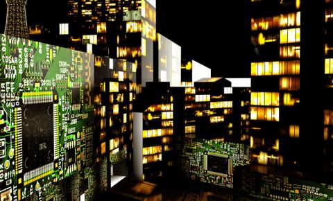
A Brave New World: PCB Data Management and the Great Paradigm Shift
PCB Data Management is the acquisition, storage, verification, usage, distribution and maintenance of all the data connected to the development of printed circuit boards or PCBs In what some refer to as the “Olden Days” of the Electronics industry, it was definitely a different time. There wasn’t much need for PCB Data, let alone anything to manage it with. Tasks such as creating schematics, BOMs, drawings, and gerber files were problematic at
Read Article
Get to Know Microvia Manufacturing Processes and HDI Substrates
Initial HDI Fabrication High Density Interconnect printed circuits actually started in 1980, when researchers started investigating ways to reduce the size of vias. The first innovator is not known, but some of the earliest pioneers include Larry Burgess of MicroPak Laboratories (developer of LaserVia), Dr. Charles Bauer at Tektronix (who produced photodielectric vias), [1] and Dr. Walter Schmidt at Contraves (who developed plasma-etched vias)
Read Article
11 HDI Materials You Need to Know
Happy Holden shows us some of the important materials used to produce high density interconnect PCB designs.
Read Article
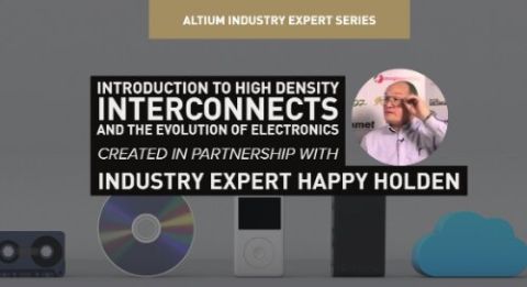
Introduction to High Density Interconnects and the Evolution of Electronics
The Evolution of Electronics Electronics is a relatively new industry, since it has been only 65 years since the transistor was invented. The radio tube was developed nearly 100 years ago but blossomed in WWII, with communications, radar, ammunition fusing (especially the radar-altimeter electronic fusing for the first atom bomb) and has evolved into the world largest industry. All electronic components must be interconnected and assembled to
Read Article
How Does the Cloud Change the DFX PCB Design Process?
Let’s face it: Engineers rarely design modern board systems on their own. However, it didn’t use to be that way. Not long ago, engineers primarily focused on form, fit, and function. Addressing those requirements was extremely difficult on its own. Constraints on cost, power, or part availability were secondary concerns. The prime directive was to get it to work. Fast forward to today, and the focus has flipped. It is a given that board systems
Read Article
Layer Management as a Circuit Board Design Tool Priority
Rome wasn’t built in a day, and the same could be said for printed circuit boards. PCBs are similar to cities in that they contain pathways connecting components. Components have dimension into the surrounding air space, as well as into the thickness of the board itself. Hidden subsystems similar to underground wiring and cityscape piping reside within the thickness of the boards. Printed circuit boards mimic cities with their layers of
Read Article
Design Rules for Large BGA Fanout
I have known people during my career who insisted on hand-routing every PCB design that they worked on. They would say that their manual routing performed better, looked better, and was just better in general. I’m not going to argue one way or the other on that, but I will say that there is one thing that can not be argued with; all of that manual routing took them a much longer time to complete than if they had used automated routers. With today
Read Article
Electronic Components Shortages in 2019, Insights from John Watson
PCB design expert John Watson shares some ideas that can help electronic component shortages & address this crisis proactively. In this episode he shares tips on how to succeed through the challenge.
Read Article
Using an IPC-2152 Calculator: Designing to Standards
If you look at modern EDA programs, there are many calculators and simulators built into these applications. But one of the areas of simulation that has lagged behind everything else is thermal simulations. Thermal calculations are important particularly in power electronics, and in high-reliability electronics, even if these systems are running lower overall power. There are other instances where we can determine the potential need for an
Read Article
Asymmetric Striplines in Your Next Multi-layer PCB
The beauty of symmetricity in art, science, and nature, in general, is something of a wonder. The visual balance between elements in a painting or drawing can make or break a piece of artwork. PCB design is as much art as it is engineering, and symmetricity plays as much of a technical role as it does an aesthetic role. Ever since its humble beginnings as a replacement for high frequency coaxial cables and waveguides, striplines are a mainstay
Read Article
Pagination
First page
« First
Previous page
‹ Previous
…
Page
250
Page
251
Page
252
Page
253
Current page
254
Page
255
Page
256
Page
257
Page
258
…
Page
260
Page
270
Page
280
Page
290
Page
300
Page
310
Page
320
Page
330
Page
340
Page
350
Next page
Next ›
Last page
Last »
Subscribe to