Skip to main content
Mobile menu
Discover
Develop
Agile
Resources & Support
Free Altium 365 Tools
Gerber Compare
Online PCB Viewer
Resources & Support
Learning Hub
Support Center
Documentation
Webinars
Altium Community
Forum
Bug Crunch
Ideas
Education
Student Lab
Educator Center
Altium Education Curriculum
Search Open
Search
Search Close
Sign In
Main menu
Home
PCB Design
Collaboration
Component Creation
Data Management
Design Outputs
ECAD/MCAD
HDI Design
High Speed Design
Multi-Board
PCB Layout
PCB Routing
PCB Supply Chain
Power Integrity
RF Design
Rigid Flex
Schematic Capture
Signal Integrity
Simulation
Software
Develop
Discover
Agile
Altium 365
Altium Designer
Education
Programs
Altium Academy
Engineering News
Guide Books
Newsletters
Podcasts
Projects
Training Courses
Webinars
Whitepapers
Learning Current Density: Don’t Pop the Balloon
One area of PCB design that probably does not get the attention that it deserves is current density. Current density in a PCB trace is much like the pressure in a balloon. You want to squeeze as much air into the balloon as you can, but if you put too much: boom! The same is true of PCB traces many times. We want the traces to be as small as possible yet carry the most current possible, and if the trace carries too much: boom! For PCBs, that boom
Read Article
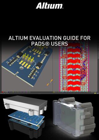
ALTIUM EVALUATION GUIDE FOR PADS® USERS
Read Article
Five Tips Guaranteed to Reduce PCB Design Time
Most engineers and PCB designers are creatures of habit. Once a roadmap has been prepared for creating successful products, that is the road most often traveled. We often don’t have the time to experiment with new techniques or look for new, innovative ways to accomplish tasks, and while that is not always a bad thing, it does not bode well if our competitors are creating successful products faster and cheaper than we are. To maintain your
Read Article
Net Clearance Rules
Designers now have the ability to set specific parameters between same net objects when placing primitives on a board. Restricting space allows you to maintain clearance for primitives, and restricting primitives of the same net to a set clearance ultimately allows greater flexibility when forcing electrical primitives to interact with other electrical objects in a specific manner. INTRODUCTION Clearance rules set requirement constraints that
Read Article
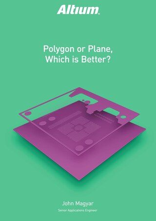
Which is Better in PCB Design: Polygons or Planes?
PCB designers have two choices when implementing large copper areas for power and ground regions: polygons or planes. Users often ask which is better in PCB designs, a polygon or a plane for implementing power and ground nets, but both design features produce similar end results. Once you’ve decided which type of structure is most useful in your PCB polygon layout, you can place the structure you need for your design using the right set of CAD
Read Article
Not That Much Force: Software for Updating PCB Layouts and Avoiding Redesigns
The other night I went to see the new Star Wars movie, “The Last Jedi," and although I really enjoyed the movie I found myself laughing out loud during one sequence. I wasn’t laughing because of the humor of the movie, or a silly looking alien—there were plenty of those to go around already. Instead I was laughing because for one brief sequence they showed some electronic circuitry that appeared to be composed of what looked like thru-hole
Read Article
The Best PCB Component Placement Software Helps You to Efficiently Finish Your Placement
Remember when we were kids and our parents gave us permission to do something fun but first we had to finish our chores? Now, taking out the garbage, folding clothes, and mowing the grass I’d prefer compared to budgeting for vacations or renovating bathrooms. Getting the chores completed lets me move on to something that is at least significantly more convenient and in many cases more fun. When I’m designing, I have similar chore preferences and
Read Article
Pass The Baton Well to PCB Design Successors
Have you ever walked into a new job, first-day energy rolling through your shoulders, only to sit down and look at the notes left from the person who last had your job and know exactly what the problem was: poor organization. Poor organization is usually pretty noticeable in any work process; however, it takes on its most detrimental final form when you are trying to train someone based on the poorly organized leftovers of someone else. Early in
Read Article
No More Wrong Ports: Implementing USB Devices In Your Hardware Design
I keep having what I like to call “Grouchy Old Man Thoughts” (GOMT). You know the type: “Why do I have to learn this new thing if what I have works for me?” or, “I wonder what it’d be like to have a conversation without them being on their phone half the time.” Well, my most recent GOMT has been that I think anyone born after the 90s is pretty lucky, technologically. They didn’t have to go through the painstaking phase before Universal Serial
Read Article
High Speed Tips and Tricks
Click the PDF above to read more about High Speed Design in this presentation. Or read the original, full-length content here: Introduction to High Speed PCB Designing: Is FR-4 the Best Board Material Choice for High Speed PCB Design? Board Layer Stackup Considerations for High Speed Board Design High Speed PCB Design Considerations: Component Shape Considerations High Speed PCB Design Considerations: Bypass Capacitor Place and Route Tips High
Read Article
Pagination
First page
« First
Previous page
‹ Previous
…
Page
309
Page
310
Page
311
Page
312
Current page
313
Page
314
Page
315
Page
316
Page
317
…
Page
320
Page
330
Page
340
Page
350
Page
360
Page
370
Page
380
Page
390
Page
400
Page
410
Next page
Next ›
Last page
Last »
Subscribe to