How to Prevent Hairline Short Circuits in Your PCB Circuit Design

What’s worse than finding a strand of hair in your pasta when you’re out on a dinner date? Finding it after it has ended up in your mouth. There are two ways to avoid awkward scenarios like this. For one, you can keep a close eye on your food and make sure it is hair free before it enters your mouth. The second is to ensure that there is no chance of a hair ending up in your food; in this case, you might need to go to a new restaurant. In PCB design, dropping a couple strands of hair won’t cause much damage, but having a single hairline short circuit on a PCB can be rage inducing in QC. The time taken to identify a single hairline short circuit and the cost of fixing it can sometimes cost more than the assembled PCB. Much like dining at restaurants that leave a hair in your food, it’s best to avoid adding hairline short circuits to your design. That being said, we’re all capable of making mistakes. You might not be able to completely avoid them, but you can employ these best practices to minimize their likelihood.
What Is a Hairline Short Circuit and How Do They Happen?
A short circuit occurs from an unintended connection between two unrelated signals. For example, when the positive voltage connection is connected to the ground signal, it is considered a short circuit. Short circuits are visible to the naked eye if the signals are connected by thick copper. This can happen if your PCBs are being produced manually rather than machine manufactured.
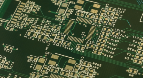
Hairline short circuits are a concern when PCBs are machine manufactured. This is because copper, that is as thin as a strand of hair, can end up connecting two different signals. This sort of short circuit can go undetected by the naked eye until the assembled PCBs are put through a series of QC tests. Unfortunately, if a short circuit is detected this late in the production cycle then it is guaranteed to cause unnecessary losses in time and raw material costs.
To understand how short circuits happens, you need to understand the general process of PCB manufacturing. PCBs are typically made of copper laminated on a non-conductive substrate. A common method to transfer the circuitry onto the PCB is through photo engraving, where a silk screen laminate containing the image of the circuit is placed on top of PCB made with photoresist coating.
The PCB is then exposed to ultraviolet (UV) light source and any areas that are not covered by the silkscreen will be etched away by an ammonia based solution. These processes are mostly automated, and an imperfection in the procedure could leave a thin line of copper connecting pads or tracks of different signals. Without thorough post-manufacturing testing, this can cause unnecessary problems later in the production stage.
Hairline Short Circuits Can Be Prevented With Proper Electrical Testing
As a self-taught PCB designer, one of my greatest and most painful lessons was not putting my PCBs through post-manufacturing electrical testing. It’s not safe to assume that your PCB manufacturer will perform all the necessary electrical checks post-manufacturing. Make sure that your PCBs pass an electrical test like the Flying Probe Test before they are sent for assembly. The Flying Probe Test moves high precision probes at high speeds over your component pads and vias to uncover any manufacturing faults and design errors.
Bear in mind that electrical testing does not guarantee a 100% error free PCB since hairline short circuits can occasionally escape testing. However, it greatly reduces the chances of a faulty PCB being sent for assembly. To further reduce your risks, you should ensure that your PCB manufacturer has a reimbursement policy for each faulty PCB that passes the electrical test. In such cases, reputable manufacturers will replace the faulty PCB and reimburse the cost of the assembled components.
Always have your PCB tested before they are assembled.
What Can Designers Do to Reduce the Possibility of Hairline Short Circuits?
While hairline short circuits are often a fault of PCB manufacturing, electronics designers can do their part to reduce their probability. Depending on how tight your design constraints are with respect to form factor or your budget, it is a good practice to opt for a larger clearance between copper connections and pads.
While there are no studies linking hairline short circuits with the clearance distance between copper traces, I have learned from experience that hairline short circuits are more likely to occur in compact and complicated PCB designs. To minimize this issue, I’ve avoided pushing the manufacturing capability of my suppliers to the limit, and I try to maximize the clearance tolerances in my designs when it is possible.
For instance, if a supplier specifies that it’s capable of handling 5 mil trace width and clearance, I’ll set my design’s clearance limit to 6 mil. When I’m dealing with new suppliers, this is a practice I always employ. As engineers, it is always prudent to test the limits of manufacturers on a smaller scale, instead of risking the whole batch of production.
When you need to access an easy-to-use PCB layout tool that includes everything needed to build high-quality manufacturable circuit boards, look no further than CircuitMaker. All CircuitMaker users also have access to a personal workspace on the Altium 365 platform. You can upload and store your design data in the cloud, and you can easily view your projects via your web browser in a secure platform.
Start using CircuitMaker today and stay tuned for the new CircuitMaker Pro from Altium.


