What Is A Gerber File and How Are They Used in the PCB Fabrication Process?
All of the pads and traces in your PCB layout will eventually need to be fabricated. How exactly do you translate your layout data from your CAD system into manufacturing instructions. The answer is simple: generate output files in an appropriate format. Today, there are multiple options for output files you can generate for your design, but overwhelmingly, your project will likely use the Gerber file format. Other available design output file formats are ODB++ and IPC-2581.
What is a Gerber file and what exactly do they communicate? We'll look at some examples of Gerber data in text and graphical format, as well as how this information is used in the PCB fabrication process by a manufacturer.
Gerber Files: The First Step in the PCB Fabrication Process
When you design a printed circuit board on a CAD system, you will see all the different materials and elements on the board represented with different styles of lines and shapes. Somehow, those graphical images need to be reformatted into data that the PCB manufacturing company can use to create the a bare circuit board. This front-end task in the PCB fabrication process is done with Gerber files.
So What is a Gerber File?
Gerber files store all of the shape and location data for every element in a printed circuit board layout. In general, each layer in your PCB layout data will be placed into its own Gerber file. The idea is that individual layers can be used to prepare stencils for each step in the fabrication and assembly process. In some cases, such as creating drill drawings or Gerber fabrication drawings, multiple layers can be merged into a single file by mirroring mechanical layers into your Gerber outputs.
In terms of the data that gets stored in a Gerber file, the data in a Gerber file is human-readable, although not necessarily human interpretable. Gerber file data is stored in an ASCII text file and it includes the following four elements:
-
Configuration parameters
-
Aperture definitions
-
XY coordinate locations for draw and flash commands
-
Draw and flash command codes
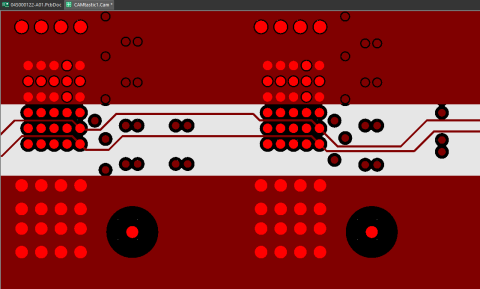
If you put all the layers together and stack them on top of each other in a combined view with a Gerber viewer application, you'll get something that looks like the simple example shown below.
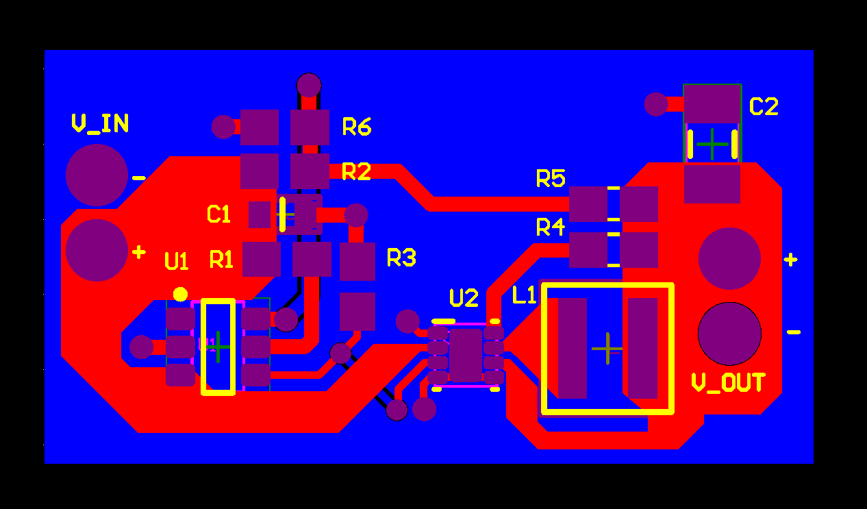
In this view, we can clearly see that the Gerber viewer's role is to recreate a view of the PCB layout as you might view it in your ECAD software. This is the view manufacturers will use to initially inspect your board before providing a quote. More specialized CAM software specifically for Gerber files can be used to perform a variety of DFM checks that mostly involve clearances; these will then get reported to you for any required updates before proceeding to PCB fabrication.
One question that you'll often see asked on forums around the internet is how to reverse engineer, or reconstruct, a PCB layout in a CAD program from a Gerber drawing file. By interpreting the information in Gerber layers (copper vs. silkscreen, etc.) along with the netlist and component data in the BOM, you could reconstruct a PCB layout just from Gerber files and other fabrication data. I've never had a need nor the inclination to do this, but there is a process for doing this in Altium Designer, included in Altium Develop.
Data in Gerber Files
Let's take a look at some examples of data in Gerber files. If you open up Gerber data in a text editor, you can read the ASCII data in the file and modify it on your own. Some manufacturers will do this by hand when correcting some design problems, and then they will check their changes with a Gerber viewer. An excerpt from a Gerber file (RS-274-X format) for a top overlay layer in a PCB layout is shown below.

There are a few things we can see that are somewhat human-readable in this example Gerber file (note the Altium Designer tag used in the header), but all the rest is not necessarily meant to be read by a human. If you really wanted, you could look up the Gerber file format guidelines from Ucamco and learn how to read each of these entries.
Viewing Gerber Files
The exact printed circuit board view that you see depends on the viewer tool you use to recreate your board. Most PCB CAD systems have the ability to generate Gerber files from design data. The round pads of a thru-hole pin will be represented in a Gerber file by a flash command along with some location coordinates. A clock line trace will be represented by a draw command code along with a series of coordinate locations for each vertex of the trace.
The reason for these command codes is that Gerber files were originally designed to drive a plotter that would create the layers of a Printed Circuit Board on film. This photoplotter would use light from a lamp or laser to expose film that would then be used to create the tooling needed by the PCB fabricator. The different codes would either flash the light, draw with the light, or move without the light. There were also codes to determine the size and shape of the light known as apertures. Although still widely used today in printed circuit board manufacturing, traditional photoplotters are beginning to be replaced by laser direct imaging (LDI) techniques where the Gerber information is imaged directly onto the circuit board materials.
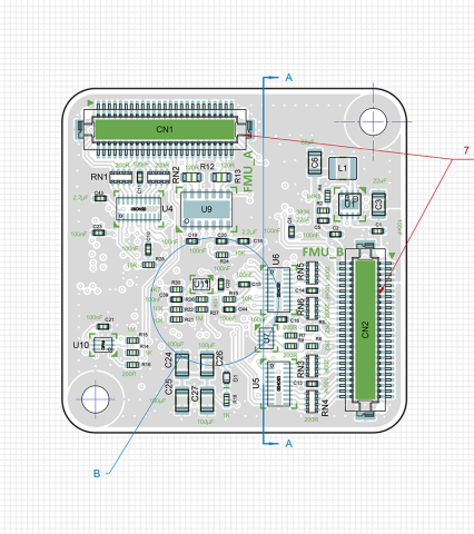
If you were to use a Gerber viewer to recreate the above information graphically, you would get the output shown below. As we can see, this information is for a silkscreen layer (top overlay layer).
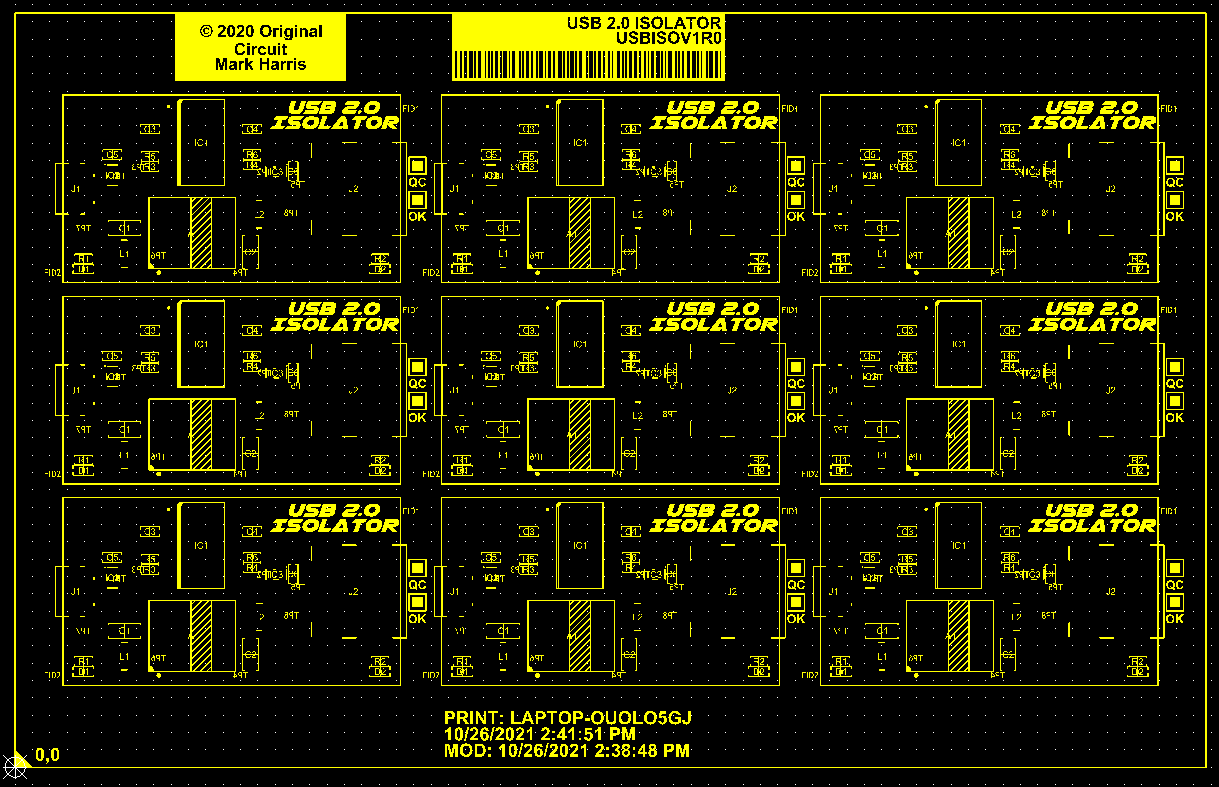
Now, because this is a silkscreen layer, can you spot the error in the Gerber drawing shown above? The board outline, connector outlines, and panel outlines are all clearly visible in this Gerber file! Normally, these would occupy their own layers and would be stored in their own Gerber files. The above problem might be intentional, such as if you wanted to use Gerbers to create a fabrication/assembly drawing, or it could be accidental due to the settings in your Gerber file generator. How can this possibly happen if each Gerber file is only supposed to correspond to one layer?
One thing you can do with your Gerber file generation tool is to mirror a mechanical layer into all of your Gerber files. This is useful for, say, placing the board outline in all of your Gerbers. You could even set up a special export that will merge a specific set of layers into a single Gerber file, which you could then use for multiple purposes. One example is creating a fabrication drawing; a Gerber drawing can be exported in a vendor-neutral file format, such as a DXF file. This then allows you to use a Gerber drawing inside another tool to create more specialized Gerber fabrication or assembly drawings.
Gerber File Formats
Over time, Gerber file formats have changed in terms of how data is structured, but they all enable the ultimate goal of reproducing the board and creating stencils for fabrication. There are three basic Gerber file formats:
- RS-274-D
- RS-274-X
- Gerber X2 format
- Gerber X3 format
The original Gerber files were known as the RS-274-D format. Those early files were only made up of the XY coordinate locations and the draw & flash commands. As PCB designers, we had to manually assign aperture codes during the Gerber file creation process. Later on, all the aperture data would be extracted into a separate file along with the configuration parameters. You had to be diligent in assigning the correct codes in order to create accurate Gerber files for PCB manufacturing.
If you are creating Gerber files today from your CAD system for PCB manufacturing, you probably are using the RS-274-X format. This version combines all four elements of the Gerber data (configuration parameters, apertures, XY coordinates, draw & flash commands) into one file. The function of each layer is defined by the file extension. You will also notice that your CAD system will more than likely automatically assign aperture positions eliminating the chance for human input errors.
Within the past few years, a new version of the Gerber format has become available that includes additional data. Gerber X2 files will include information such as the layer function of that file, object functions such as pad types, locations of impedance-controlled traces, and much more. Regarding layer function, this information will be written inside the file, rather than using a specific file extension to denote layer type. The goal is to enhance the Gerber format to make it more like a database such as ODB++ while still having the legacy ability to drive photoplotters and LDI systems.

What Does This Mean For You?
Most PCB design software packages can at least export Gerber files, even if they do not have a built-in Gerber drawing viewer or Gerber compare feature. As a PCB designer, your job is to make sure you understand the basic Gerber file extensions, what data is contained in different Gerber files, and review Gerbers briefly before sending them in for fabrication. Some manufactures may still require separate aperture lists or other data files, and you need to know what those files do and how to create them. A quick review of your Gerber drawing files before sending off to fabrication can help you spot any error that might delay fabrication or cause the finished board to totally fail.
Today, it's never been easier to understand what is a Gerber file and to share your PCB fabrication data with your manufacturers. Altium Develop includes a Gerber file viewer thanks to its built-in CAM tools, and it will automatically export your Gerber data in RS-274-X or Gerber X2 file formats. When you’ve finished your design, and you want to release files to your manufacturer, Altium Develop makes it easy to collaborate and share your projects.
Whether you need to build reliable power electronics or advanced digital systems, Altium Develop unites every discipline into one collaborative force. Free from silos. Free from limits. It’s where engineers, designers, and innovators work as one to co-create without constraints. Experience Altium Develop today!


