


DFM in Your PCB Layout

At a Glance
PCB design reviews should focus on DFM constraints to ensure a design will be manufacturable. Focus on these DFM requirements in your PCB layout.


Building a board means conforming to the manufacturing process for your layer stack and material selection. At some point, you will have to design the connections on your PCB, and even these have specific requirements as that are intended to ensure manufacturability. In this section of our DFM crash course, we'll look at some of the basic DFM constraints on conductive elements in a PCB, as well as the development of the surface silkscreen/solder mask layers for DFA.
Successful DFM in the PCB layout starts by setting your design rules to account for important DFM constraints. The DFM rules shown below reflect some of the contemporary design capabilities one would find at most manufacturers. Make sure the limits you set in your PCB design rules do not violate these limits so that you can make sure you comply with most standard design limitations.
Strategizing Your PCB Layout
With your material selections finalized, it is now time to dive into the specific details of your PCB layout. While individual engineering workflows might differ from one designer to the next, there are a number of primary design considerations that have a need for precise DFM requirements to consider a board 100% ready for manufacturing. In the following sections you will learn the specifics of strategizing your PCB layout including SMT and through-hole specifications, silkscreen documentation, solder mask applications, and more.
Via Size and Clearance Requirements
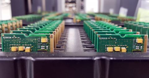
Pro designers use multilayer PCBs with routing on two layers, which requires the use of vias. Vias are a critical part of every PCB design and are responsible for transmitting electrical current between layers. When designing plated through-hole vias, it is recommended to maintain an 8:1 aspect ratio between the hole diameter and the via length. The table below shows a set of standard drill sizes (in mils):
|
|
|
|
|
|
|
|
|
|
|
|
|
|
|
|
|
|
|
|
|
|
|
|
|
|
|
|
|
|
|
|
|
|
|
|
Standard vias should maintain minimum clearances from adjacent conductors. The clearance will depend on the particular processing capabilities of the fabrication house, as well as the need for specific clearances as required for certain types of PCBs (such as high-voltage boards). There is a via-to-via clearance that will limit the allowed density of vias, with typical drill hole wall to drill hole wall clearances of being as large as 10 mils. These requirements will limit how densely connections can be routed between layers as well as the density of stitching vias when tieing planes or polygons together.
Through-hole or SMD?
Choosing through-hole components or surface mount devices (SMD) will have a direct impact on your overall costs and manufacturing time. It is recommended to stick with SMD for modern board designs as this results in quicker board turnarounds and higher reliability. Most components that would be needed for a modenr design are manufactured as SMD components. Some exceptions include connectors, which are often availalable as SMD or through-hole components. To keep production costs lower in a design and to ensure minimal solder passes are needed, it is desirable to only have placement on one layer, even in cases where both types of components are mixed in the same type of design.
Annular Rings
The annular ring is usually defined as the difference between the desired pad diameter and the corresponding drill diameter, although this is not completely correct. The classic definition I just noted is referring to the landing pad on a via. The reality is that the annular ring quite different from the via landing pad size; it refers to the leftover copper ring around a drilled hole after the hole is drilled, etched, and plated with copper. The drill does not always strike the pad perfectly dead center due to wander during manufacturing. The result is that the drill could be slightly off-center and would leave some copper around the via hole.

From the above image, we can see that the annular ring width for a perfectly fabricated via would obey the following formula:
Annular Ring Width = (Diameter of the pad – Diameter of the hole) / 2
To ensure the board comply with IPC reliability standards, The pad diamater should be 8 mils (IPC Class 2) or 10 mils (IPC Class 3) larger than the via drill hole diameter. This is a conservative limit that will ensure there is almost always some annular ring around the finished via.
Via Aspect Ratio
Aspect ratio of a via is the ratio between the depth of the via and the diameter of the drilled hole (after applying plating). The aspect ratio of vias should be kept low enough to ensure high yield fabrication of these structures. For more advanced designs, like HDI PCBs that use microvias, the aspect ratio limit can be very small, reaching 1:1 or smaller. Make sure to check your fabricator's capabilities before you start adding vias into the PCB layout. You can set the limits on via sizes inside your PCB design rules.

Via-in-Pad and Micro Vias
When connection densities become very high, such as in a BGA with fine pitch, it is possible to place the via directly in the landing pad for a component. Via-in-pad design allows for close placement of components because vias do not have to placed some distance away from their connecting landing pad. Via-in-pad designs require some fill with conductive or non-conductive epoxy, followed by capping and plating to protect the interior of the via structure.
Via-in-pad is used with through-hole vias in cases where mechanical drilling is still possible, the limit of which can be as small as 8 mils. When component density is extremely high, HDI design techniques are needed to make connections to inner layers. This is a more advanced topic that is discussed in our other eBooks.
Should Vias Be Tented?
A tented via is a standard via that has its surface layers covered with soldermask so that no copper is exposed It is typical to define small vias (12 mils or less) as tented. Larger vias may require cap and fill before they can be tented with solder mask. Vias are tented for a variety of reasons, and it is a good idea to tent them when they are very close to landing pads on SMD components. The example below shows one instance where it is necessary to apply tenting due to the proximity between vias and a bank of solder pads on an SMD component. In this case, if the vias were un-tented, it's possible for solder to wick through these onto the back of the board, possibly causing a short circuit.

Although there are assembly concerns, there may still be a reason to leave vias un-tented. For example, if a specific via is desirable for use as a test point, then it needs to be accessible with a probe, so the solder mask will need to be removed from that via. Testing will be discussed more in the next chapter in this series.
Blind and Buried Vias
Similar to through-holes, blind and/or buried vias (BBV) are holes that connect one or more layers. In this process, a blind via connects an outer layer to one or more inner layers but not to both outer layers, and a buried via connects one or more inner layers, but not to an outer layer. The image below shows an example cross-sectional view of a 6-layer PCB with blind and buried vias:

Do not just assume that your fabricator will be able to produce every possible combination of blind and buried vias. Mechanically-drilled and laser-drilled blind and buried vias must be set into specific layers to ensure successful fabrication, they cannot be placed on arbitrary layer pairs. Make sure you contact your fabrication house first and obtain some guideance on the use of blind and buried vias in a PCB layout.
Necking a Trace
In some cases, it is necessary to neck down a trace in order to route into a landing pad for a component. A necked trace (sometimes called neck-down) connects to a pad and runs at least 0.010” away from the pad before tapering out to the large trace width.
For controlled impedance traces, such as would be needed in high-speed designs, it is generally a bad idea to apply necking as this creates an impedance deviation. Instead, us thinner layers if you need to maintain a smaller width. Components for these designs will tend to have smaller landing pads anyways, so they will not need necking if the stackup and traces are sized properly.

Placing and Orienting Your Components
With your preferred component types established, it is now time to decide how to efficiently place and orient those parts on your board. This process will have a large effect on how you utilize the available space on your board layout, and can be one of those most challenging steps in your design process. Below you will find specific recommendations on how to optimize your component placement to be both manufacturable and capable of meeting your specific design requirements.
Before going into the specifics of component placement and orientation, there are several general guidelines to keep in mind:
- Orient components with I/Os and similar footprints in the same direction.
- Try to place all your SMT components on the same side of the board, and all the through-hole components (if mixed) on the top side of the board.
- When you have mixed technology components (SMT and PTH), manufacturers might require an extra solder process to place bottom components.
- You should terminate all lands with only one trace.
- When you specify a chip under a device, this can make inspections, rework, and test more difficult.
- All components used on the wave solder side of an assembly should first be approved by your manufacturer for immersion in a solder bath.
With the information presented in this chapter, you are now well-equipped to begin your component placement and orientation process to meet fundamental manufacturability requirements. Now that your design is well on its way to completion, it is time to finalize the board layout process by configuring your test point requirements in the next chapter.
- Go to Part 4: Board Cleanup and Testing Requirements
When you're ready to start your design and you want to make sure you meet every DFM requirement for your PCB layout, use the design and layout features in Altium Designer®. Once your design is ready for a thorough design review and manufacturing, your team can share and collaborate in real time through the Altium 365™ platform. Design teams can use Altium 365 to share manufacturing data, project files, and design reviews through a secure cloud platform and in Altium Designer.
We have only scratched the surface of what’s possible with Altium Designer on Altium 365. Start your free trial of Altium Designer + Altium 365 today.

About Author
Related Resources
Table of Contents
Design to Release, Without the Friction
- Keep reviews tied to the right version
- Reduce handoff confusion and rework
- Spot sourcing and release risk earlier
- Work solo, share when needed
Get Started
Thank you, you are now subscribed to updates.


