


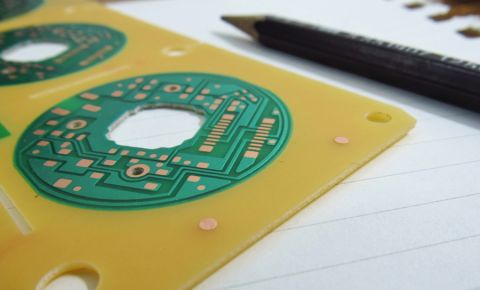


Do You Need an IPC-D-356 Netlist?

At a Glance
See why your PCB design outputs package will need an IPC-D-356 netlist.


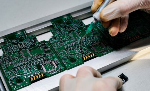
When your PCB fabrication files are sent in for review with a manufacturer, they need to review the physical structure of your copper and mask layers, as well as the electrical connections between different sections of copper. All those smart data formats like ODB++ and IPC-2581 enable checking of net connections with an integrated netlist. The most common data format sent for fabrication remains Gerber files, along with the associated drill files and documentation.
This is where an IPC-D-356 netlist format comes into play. While this is not required to fabricate a bare PCB, it is an essential file as part of an output package so that the design can be qualified for production. Let's look more at this format and how to quickly generate one inside Altium.
When Do You Need an IPC-D-356 Netlist?
This netlist format is not required to fabricate a PCB. All that is technically required is the Gerber outputs and drill files. Anything outside of this information can be guessed by the fabricator, or you can tell them to fabricate using the files as supplied.
However, if you want your fabrication house to review the copper connections in your design and identify any short circuits, then you will need to supply a netlist. The most common of these formats is the IPC-D-356 format, as it is a vendor-neutral, human-readable netlist format. These text-based files list the following information:
- Every net contained in a PCB layout
- The pin/pad/testpoint connected to each net
- The coordinates and layer of each net connection
- The associated drill spans for holes connected to each net
A sample of the IPC-D-356 netlist for our recent NFC Reader project is shown below. The sample shows the header block followed by some of the netlist entries. Learn more about this project and access the design files in this linked article.

From this sample, you can see that the netlist is indicating connections first on all the pins on U1, which happens to be the ESP32 chip in the NFC reader design. Then it moves onto the other components (J1, U5, etc.). By using the IPC-D-356 file, a fabrication house can determine opens/shorts and thereby verify the copper in your Gerber files matches the et connections defined in your schematics.
About the IPC-D-356 Format
The IPC-D-356 standard comes in two revisions (A and B), with revision A most commonly supported in CAD software. Before IPC-D-356, all PCB CAD tools used proprietary formats to textually describe the graphical information found in IPC-D-356 (net names, pad/pin connections, etc.). Electrical testing could then be planned based on the CAM-extracted netlists from Gerbers, but this is error-prone because Gerbers contain no net names or logical relationships. In contrast, the IPC-D-356 format lists designators and clear pin numbers, as shown above.
By receiving an IPC-D-356 file, the fabrication shop can:
- Confirm no opens or shorts exist in the manufactured PCB
- Validate that all connections match the design’s intended nets
- Catch errors such as missing internal connections, reversed pins, or layer-to-layer discontinuities
Today, we can get around the requirement for this netlist format by using an intelligent data output format, like ODB++ or IPC-2581. These file formats offer much greater levels of intelligence by integrating all the standard PCB design outputs into a single archive (or a single file, in the case of IPC-2581). The major CAD vendors, including Altium, currently support the ODB++ and IPC-2581 file formats, although not all manufacturers have processes in their CAM departments to use these formats.
Generating an IPC-D-356 Netlist
Altium supports the creation of IPC-D-356 netlist files as a standard output from an OutJob file. To generate an IPC-D-356 file in Altium, follow these steps:
- Open the OutJob file for your project
- Add a new fabrication output; select the "Test Point Report" option as the source
- Right-click on the new Test Point Report output and choose "Configure" to access the Fabrication Testpoint Setup dialog.
- Check the IPC-D-356A checkbox.
- Assign the report to an Output Container and configure the export location/name
- To generate the IPC netlist file, click on the Generate Content option in the Output Container
This will create a .ipc file that contains the netlist for your project. This file will be named based on the configuration you apply in Step 5.
If you have Gerber files with a corresponding IPC netlist, you can also inspect the Gerber files using the CAMtastic! viewer in Altium. Follow these steps:
- Create or open a CAMtastic document
- Import the IPC-356 Netlist: Load your Gerber files, NC Drill file, and netlist into the CAM document using File -> Import
- Extract the netlist information from the loaded Gerber/NC Drill data by selecting Tools » Netlist » Extract.
- As an option, you can rename the nets to match the imported IPC netlist information using Tools -> Netlist -> Rename Nets.
- Compare the imported IPC-356 netlist with the extracted netlist, select Tools » Netlist » Compare.
For more detailed guidance on generating IPC-D-356 documentation, you can refer to this knowledge base article.
Whether you need to build reliable power electronics or advanced digital systems, use Altium’s complete set of PCB design features and world-class CAD tools. Altium provides the world’s premier electronic product development platform, complete with the industry’s best PCB design tools and cross-disciplinary collaboration features for advanced design teams. Contact an expert at Altium today!
About Author
Related Resources
Related Technical Documentation
Table of Contents
Design to Release, Without the Friction
- Keep reviews tied to the right version
- Reduce handoff confusion and rework
- Spot sourcing and release risk earlier
- Work solo, share when needed
Get Started
Thank you, you are now subscribed to updates.

