Can CPLDs Be Used in Mixed-Signal Applications?

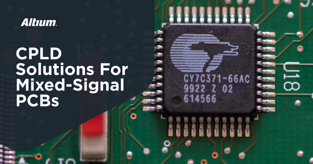
Complex programmable logic devices (CPLDs) are digital devices with some level of silicon programmability by the system designer, sitting somewhere between an MCU and an FPGA. Traditionally, CPLDs are only used in digital applications, where logic is implemented on a dedicated chip without the need to run firmware for an embedded application. This means logical functions can be instantiated permanently in a chip on silicon, reducing the overall system complexity.
While CPLDs perform logic functions outside of an MCU in a highly integrated package, they can be a struggle to use in mixed-signal applications. In these systems, logical conditions are applied based on some measurement of an analog signal; while a CPLD can easily perform the logic functions they cannot perform the analog signal measurements required in a compact mixed-signal application.
Fortunately, there are other approaches that can be used with CPLD, or a new type of mixed-signal IC can be used to implement CPLD functionality with analog measurements. This article will show how these mixed-signal applications work, both with a CPLD and with a newer mixed-signal IC.
What is a CPLD?
A CPLD is a programmable digital component that can perform multiple logic functions within a single component. They are integrated circuits that eliminate the need for discrete logic gates and external memory as all functions are written directly to the device. Logic functions in a CPLD can be chained together and performed in sequence, eventually producing a specific set of logic outputs given a set of logic inputs.
The primary component in any CPLD is known as a macrocell; the function and sequencing of these components is what a systems designer programs into a CPLD to perform the desired logic functions. Macrocells include several components that work together to implement combinational and sequential logic functions:
- Product logic (based on AND gates) that generates product terms from the input signals.
- Sum-of-products logic (based on OR gates), allowing implementation of complex Boolean functions.
- D flip-flop/register for sequential logic and storage of state information
- Look-up tables (LUT) for low-latency logic operations
- Multiplexers that provide signal routing flexibility allowing selection between combinatorial output (bypassing the flip-flop), registered output (via the flip-flop), or feedback
- Clocks and timers, including asynchronous set/reset functions for the flip-flop
- Output buffer that drives signals off-chip, which may support bidirectional I/O
The exact configuration and complexity of these components varies between different CPLD families and manufacturers, but these elements form the fundamental building blocks that give macrocells their flexibility in implementing both simple and complex digital logic functions.
Analog Signals With CPLDs
Because CPLDs do not include analog interfaces, the only way the state of an analog signal could be used with a CPLD is with some external analog circuitry that can sample or measure an analog signal. This requires two options:
- An ADC, or the ADC pin on an MCU
- A comparator with hysteresis
- A DSP chip or DSP algorithm in an MCU
For simple threshold-based sampling with some built-in noise tolerance, a comparator with hysteresis would be used to sample the analog signal. For more complex operations on an analog signal, an ADC/DSP approach is needed. The MCU output in this case could be a small number of bits indicating a specific state or measurement of the analog signal. This output could then be fed to the CPLD for further logic operations.
The most common approach is to use the comparator with hysteresis as this allows logic operations to be performed in the CPLD without requiring an MCU. The reason the ADC or DSP approach is not used more often is that the logic in the CPLD can also be implemented in the MCU. Another approach that would give the low latency of the CPLD would be to use everything in an FPGA instead of the MCU.
Programmable Mixed-Signal IC
What if you could take the ADC/DSP approach with a CPLD but without requiring an MCU for any logic operations? This can be accomplished with a programmable mixed-signal IC. These components integrate analog I/O and digital I/O into the same package with the logic operations performed using macrocells, similar to a conventional CPLD.
With an integrated analog front end, an analog signal can be sampled with common inputs found in an analog front-end:
- Comparator with programmable reference voltage and hysteresis
- ADC (or a DAC on the output side)
- Programmable gain amplifier (PGA)
For example, take a look at the block diagram for the SLG46826 from Renesas. In this block diagram, the macrocells provide the logical functions, primarily through flip-flops, delay counters, and LUTs.
SLG46826 block diagram
The system designer develops the analog signal flow and logic using a vendor IDE, just as would be the case in a conventional CPLD. Although not requiring an interface to an MCU, a programmable mixed-signal IC may have an I2C or SPI interface which allows a connection to an MCU or FPGA if needed.
If you’re looking for mixed-signal processing with the same approach used in CPLDs, try using the GreenPAK programmable mixed-signal matrix products from Renesas. GreenPAK provides a set of hardware components and associated software solutions that help systems designers quickly implement compact mixed-signal solutions while eliminating many complex analog circuits. To see how to use GreenPAK and develop a new solution, check out the Solution Cookbook and documented code examples.
Whether you need to build reliable power electronics or advanced digital systems, use the complete set of PCB design features and world-class CAD tools offered by Altium to implement your GreenPAK solutions. Altium provides the world’s premier electronic product development platform, complete with the industry’s best PCB design tools and cross-disciplinary collaboration features for advanced design teams. Contact an expert at Altium today!
