


UART vs. SPI vs. I2C: Routing & Layout Guidelines

At a Glance
If you’ve never worked with an MCU and programmable ICs, here are some routing and layout guidelines on I2C vs. SPI vs. UART.


If you’re building a dev board for your project or using a common MCU, you’ll find many protocols for communicating other active components. Standards like USB and Ethernet are built into most controllers for working with computer peripherals. Still, protocols like I2C, SPI, UART, and others are used to interface with downstream MCUs or programmable ICs. The differences between SPI vs. I2C vs. UART buses are simple, and any designer working with an MCU should know how to follow routing and layout guidelines for these protocols.
These protocols are slower speed signaling standards, so you almost always won’t need to worry about things like impedance control or transmission line behavior if you are working with these protocols. However, some important design points must be considered when ensuring your bus lines’ signals are read correctly by your receivers. There is also the matter of addressing, but the particular product and your code can handle this point. For now, let’s look at how these three common protocols can be used in your PCB layout, establish some layout/routing guidelines, and touch on some important points to maintain signal integrity.
Differences Between I2C vs. SPI vs. UART and their Layout Guidelines
Everything from 8-bit to 32-bit MCUs will use at least one of these protocols alongside GPIOs for programmability and sending signals to simple peripherals. These three serial protocols are bus protocols; I2C and UART use addressing schemes, while SPI is addressless. Although SPI is addressless, it is a bus protocol and can still be used to select downstream devices to receive data.
I2C Protocol Routing & Layout Guidelines
I2C (pronounced I-squared C, or sometimes IIC for inter-integrated circuit) uses two lines (standard, fast, and fast-plus modes) to control other devices; one line is a clock line (SCL), while the other is a data line (SDA). It comes in three modes, which are summarized in the table below. Note that the rise/fall time values assume the typical series resistors are installed at the I/Os.
|
Mode |
Data rate/clock speed |
Max. rise/fall time |
Min. rise/fall time |
Directionality |
|
Standard |
100 kHz |
1000 ns |
- |
Bidirectional |
|
Fast |
400 kHz |
300 ns |
20 ns* |
Bidirectional |
|
Fast-plus |
1 MHz |
300 ns |
20 ns* |
Bidirectional |
|
High speed |
3.4 MHz (100 pF bus) 1.7 MHz (400 pF bus) |
120 ns** |
15 ns** |
Bidirectional |
|
Ultra-fast |
5 MHz |
50 ns |
25 ns |
Unidirectional |
*Assumes VDD/VCC = 5.5 V. Scales down linearly if VDD/VCC is lower
**Divide these values by 2 for the clock line
Note that ultra-fast mode is the only mode where communication is used for downstream write operations only. This mode is also important as it helps us see when the bus impedance will need to be matched, which in practical terms is almost never. If we take a very conservative 10% limit on the critical line length, we find that the crucial length in these lines is 0.32 m, which is much longer than the size of most boards that will use I2C. If we use the knee frequency for the minimum rise/fall time with a 10% limit on critical length, we come to a much longer value of 0.92 m. We should take the more conservative number of 0.32 m for ultra-fast mode; any I2C line shorter than this value will not behave as a transmission line, and we only need to worry about the termination scheme.
The important points in termination are to select the right pull-up and series resistors. The pull-up resistors and the capacitance of the VDD/VCC line bus form a discharging and charging RC circuit, which is what provides a signal to the receiver when the driver switches. The pull-up resistor values (Rp) for the signal and clock lines must obey the following inequality:

Note that the number in the denominator above is defined for a 30% to 70% transition time, which is the standard in the I2C specification. For a 10%-90% transition time, replace 0.8473 with 2.2. This will further limit the value of the pull-up resistors.

The bus capacitance is determined using the standard formulas for the VCC bus impedance, which could be calculated using the same equations you would use for a transmission line (either microstrip or stripline). You can then solve for the bus capacitance using the impedance and the propagation delay for the line. If you're not in the mood to do that calculation, there are I2C bus capacitance calculators you can find online. Finally, the series resistors are optional under the I2C standard, although they can be included to protect the devices from voltage spikes and slow down the rise/fall times. Look at Fig. 46 on page 59 of the I2C standard to determine the right series resistor value to pair with your pull-up resistor value.
SPI Protocol Routing & Layout Guidelines
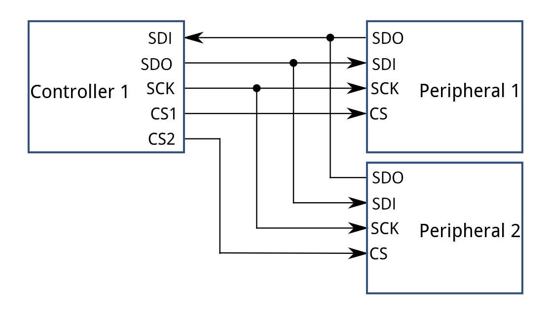
The SPI protocol is similar to I2C. A total of 4 lines are used in this bus, and components can be arranged in two possible modes. If a single controller device is used to trigger a single downstream device, the topology is simply point-to-point. Triggering multiple devices depends on the number of chip-select outputs provided by the driver (standard mode). The second mode uses daisy-chaining, where a single device-select output successively triggers each device in the daisy chain.
In the example above, our controller has two chip-select outputs which are used to trigger when the peripherals will receive and accept data from the host. When serial data is output from the controller, the required peripheral also needs to be activated by the controller during a data frame so that the peripheral will accept and read the data. This is programmed in the controller’s logic. For example, if a microcontroller or FPGA is used as the controller, it will be implemented in the code for the device’s application.
Unlike I2C, the various signaling parameters in SPI are highly configurable. The RC discharging method with the trace capacitance shown above can control the output current and rise/fall times from your interface. SPI is a push-pull interface, and power is not being drawn through a pull-up resistor. The rise time is dominated by the external capacitance and the driver's output impedance. The SPI spec on your host controller might give a specific rise time for a specific current draw into the bus for a specific total capacitance (maybe 50 or 100 pF). For example, in the SPI bus on a PIC32 MCU, the output transition time is specified as 5 ns for an external capacitance of 50 pF. So if we drop to 10 pF, we would expect the rise time to drop to 1 ns for a given current output and voltage level. In that case, you now have a 0.6-inch length allowance (rough approximation with a very conservative 10% limit on unmatched lengths). You can then use a series resistor to terminate the driver’s low impedance output in the event the line becomes very long for a short rise time.
UART Protocol Routing & Layout Guidelines
The universal asynchronous receiver transmitter (UART) protocol is similar to I2C and SPI. These interfaces have a maximum data rate of ~5 Mbps. UART devices are also easy to work with as there is no clock sent between devices; everything is asynchronous. Note that each UART device’s internal (system) clock must run at some multiple of the baud rate (i.e., each bit is sampled N times). Only two wires are used for communication between a single controller device and a single downstream device.
Note that the data format, signal levels, and baud rate of a UART device are configurable with an external driver circuit. Whether or not you see high-speed signal behavior depends on whether you're transmitting with RS-232 or RS-485 signal levels. UART signals at RS-232 levels are normally done without termination because the edge rates are slow. However, RS-485 with UART signals typically requires termination resistors. Follow the standard high-speed design guidelines for determining when termination is needed by looking at the transition to transmission line behavior (see the article I linked above).
A typical termination method to reduce overshoot in the event it occurs is to apply series termination. Note that UART may idle at high or low levels, and pull-up resistors may be needed to set the required idle level; be sure to check your component specifications before adding pull-up resistors.
You can read more about the difference between timing in synchronous and asynchronous buses in this 2018 AltiumLive presentation by Max Seeley.
Summary
If SPI and UART rules seem a bit vague, it’s because you have more freedom to design your interface at the firmware level. Once any of these standards run at fast edge rates, they are susceptible to crosstalk, just like high-speed signaling standards. However, because you have plenty of flexibility in your specification, you can usually design traces to have lower inductance and reduce inductive crosstalk. You have some flexibility in routing these signals and making them very easy to work within your next digital system.
When designing digital systems with common signaling standards, you can design for the differences between I2C vs. SPI vs. UART layout guidelines with the design rules in Altium Designer®. The Layer Stack Manager and the integrated 3D field solver from Simberian use your board geometry and trace geometry to extract the parasitics in your signal lines and help you determine impedances if your signals ever get too long lengths or high speeds.
Altium Designer on Altium 365 delivers an unprecedented amount of integration to the electronics industry until now relegated to the world of software development, allowing designers to work from home and reach unprecedented levels of efficiency.
We have only scratched the surface of what is possible to do with Altium Designer on Altium 365. You can check the product page for a more in-depth feature description or one of the On-Demand Webinars.

About Author
Related Resources
Related Technical Documentation
Table of Contents
Design to Release, Without the Friction
- Keep reviews tied to the right version
- Reduce handoff confusion and rework
- Spot sourcing and release risk earlier
- Work solo, share when needed
Get Started
Thank you, you are now subscribed to updates.

