Common PCB Assembly Defects You Should Know

At a Glance
In this Blog, Tara gives a list of the most common assembly defects, some that PCB design can influence and some that are related specifically to the assembly process itself.


PCB designers are the architects behind the technology that powers our modern electronics, balancing a host of requirements, navigating a complex layout that is as much art as it is science. Yet, even the most carefully designed printed circuit boards can face defects during PCB fabrication and assembly. In this blog we will look at an overview of the most common assembly defects, some that PCB design can influence and some that are related specifically to the assembly process itself. Then we will drill down into a specific defect, warpage of the PCB and components and look at how PCB design can influence this defect. Looking forward to future blogs, we will examine these defects from a manufacturability perspective to help bridge the gap between PCB design and assembly.
Common PCB Assembly Defects
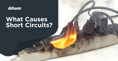
Solder Bridging/Short Circuits: This defect occurs when solder connects two or more conductive features, causing unintended electrical connections. This could be between adjacent pins, pads or circuit traces.
Insufficient Solder: Inadequate solder can lead to incomplete or weak solder joints which in turn leads to poor electrical connection. This can present as an intermittent or open connection.
Solder Balling: Solder balls are small, unintended solder deposits that can occur during reflow soldering resulting from incomplete melting and flow of solder paste. These can lead to shorts if they are in sensitive areas of the PCB.

Solder balls appear when solder paste becomes unmixed or is stored incorrectly. [Image Source: User John U, stackexchange.com]
Tombstoning: This is when a surface mount component stands on one end due to imbalanced solder reflow, resulting in poor electrical connection. This defect is often caused by temperature differences during reflow.
Lifted or Missing Pads: Pads can become detached during assembly resulting in non-functional components.
Component Misalignment: Surface mount components may be misaligned or skewed during placement leading to solder joint defects or open connections.
Cold Solder Joints: Cold solder joints are brittle weak connections that result when solder does not flow properly during reflow, often due to insufficient heat or improper flux activation.
BGA Soldering Issues: Ball grid array (BGA) components can suffer from solder ball defects, open connections, or solder voids beneath a component, which can lead to poor connectivity and reliability issues.
Component Polarity Reversal: Errors in component placement or orientation can result in incorrect polarity, resulting in reverse voltage connection and potential damage.
Excessive Solder Paste: Applying too much solder paste during stencil printing can cause solder shorts and other solder related defects.
Insufficient Solder Paste: Insufficient solder paste can lead to incomplete or weak solder connections, especially for fine-pitch components.
Insufficient Solder Fillets: Solder fillets that do not adequately from around components leads or pads resulting in weak connections.
Solder Ball Residues: Solder balls left on the PCB surface after reflow can cause short circuits and other issues.
Missing components: Components missed during placement due to equipment or operator errors.
Warped or Bent Components: SMT components can become warped or bent during reflow, affective their placement and solder joint quality.

High warpage in the PCB can result in SMT package warpage. [Image Source]
Warpage, Mitigate the Risk
PCB designers can take several measures to minimize component and PCB warpage, which can contribute to defects like solder balling during PCB assembly. Here are few ways the printed circuit board design can impact and potentially prevent warpage:
Component Placement and Footprint
- Carefully select component locations and orientations to minimize stress.
- Avoid placing heavy components in sensitive areas.
- Use components with flat or coplanar leads, which tend to exert less stress on the board.
- Design appropriate component footprints that accommodate thermal expansion and contraction during soldering.
- Ensure that component pads are large enough to provide mechanical stability and solder joint strength.
- For heavy or tall components, consider additional mechanical fastening methods such as screws or standoffs to provide stability and prevent warping.
- Aim for a symmetric board layout, distributing components and features uniformly to prevent stress in specific locations.
- If using copper planes, add thermal relief connections for components with large ground or power connections to prevent the board from wrapping during reflow soldering.
Board Stackup
- The PCB stackup should balance the copper distribution on both sides of the board to minimize warpage.
- Opt for balanced stackups with symmetric copper weights and dielectric thickness across the stackup.
- Select printed circuit board materials that have good dimensional stability and low coefficient of thermal expansion (CTE).
- Consider using materials designed for high-temperature applications if your design requires it.
Thermal Considerations
- Be sure that components generating significant heat have proper thermal management solutions. Heat sinks, vias, or dedicated copper planes can help with this.
- Distribute heat-generating components evenly across the board to prevent localized heating and warping.
- Avoid placing densely populated heatsinks or connectors near the PCB’s center. These may exert uneven forces and contribute to warping.
I will wrap up this blog with a piece of advice. It is important to engage with both fabrication and assembly during the design process. There are so many examples of items as simple as solder mask color that impact yields which impact pricing and lead time. Bringing together design, fabrication, and assembly to collaborate and communicate throughout the manufacturing process will set a design up for the best chance of first pass success.
When you're ready to create your PCB layout with best DFA practices for SMT assembly, use the design and layout tools in Altium Designer®. To implement collaboration in today’s cross-disciplinary environment, innovative companies are using the Altium 365™ platform to easily share design data and put projects into manufacturing.
We have only scratched the surface of what’s possible with Altium Designer on Altium 365. Start your free trial of Altium Designer + Altium 365 today.
About Author
Related Resources


Related Technical Documentation

Thank you, you are now subscribed to updates.


