Five First Pass Perils in PCB Prototyping Runs

The first pass prototyping run for a new design is where its functionality really gets put to the test. The functionality of your PCB depends on the quality of the design you create in your CAD tools, but sometimes the prototype just doesn't function as intended. There are many possible reasons for this, which could be related to your design choices, the capabilities of your manufacturer, or both.
Founders without hardware experience might underestimate the challenges involved in mass manufacturing hardware. Your investors may be pressuring you to move immediately to 100,000 units on your first pass. The reality is simple: if you can't get the board perfect when producing QTY 1, you will never scale up to QTY 1,000,000. Before scaling, make sure you understand what can create defects in your first-pass prototyping run.
What Could Go Wrong in Your First Board Spin?
The first time your board passes into prototyping is probably the first time every single one of your design decisions will be put to the test. Prototyping gives you a chance to identify any of the most important issues that could reduce your first pass yield and thus derail your attempt at scaling.
In the event you get your prototypes or first-pass run back from your assembler, and you find that the boards are defective, there could be any number of reasons this occurs. What I've outlined below shows four common reasons a prototype design might fail to function as expected.
Shorts or Bridging Under a BGA or LGA
Problem - Since so many advanced designs use components in BGA, it makes sense to start here. BGA footprints use a set of solder balls to define connections to the component package. Unfortunately, soldering of BGAs can lead to defects that may not be obvious during inspection, specifically short or open circuits. The set of possible BGA-related defects leading to shorts/opens includes:
- Bridging across SMD pads
- Incomplete wetting and/or insufficient solder (head-and-pillow)
- Solid solder joints but incorrect electrical connections
PCB assemblers who work with BGAs will perform X-ray inspection as a standard practice. X-ray inspection will rule out the first two defects, but it cannot rule out the last point. This last point relates to the PCB footprint, which may have been created incorrecty. Note that the same points apply to LGA packages.
Solution - Ensuring quality and yield in BGA soldering is the responsibility of your assembler. Assuming the PCBA does not have soldering defects, the problem could originate in your BGA footprint. Specifically, when you create the land pattern data for your BGA make sure you pay attention to the part orientation in the drawing. Sometimes the pad arrangement is shown as a bottom view, but typically it is a top view. Don't assume, check the specific view orientation in the footprint before making pad assignments in your BGA footprint.

Rotated Parts
Problem - A part is mysteriously rotated by 90 or 180 degrees during assembly, and in most instances this makes the board unusable. While the problem can be corrected with some simple rework, it's still a time waster and it could incur some additional cost to manually rework the boards. This occurs because the component pinout is symmetric and the footprint does not contain a polarity marker on the silkscreen layer.

Solution - Make sure polarity indicators (Pin 1 markers) are present for any components that have a polarity. There are three broad groups of components where this applies includes:
- Polarized passives (diodes, electrolytic capacitors)
- Symmetric integrated circuits
- Symmetric connectors
Your assembler should perform a review of the board before placing the design into the solder process, and typically this will be caught during a review. Just to ensure that there is no ambiguity, make sure that checking for Pin 1 markers is part of your PCB design review checklist.
Insufficient Annular Ring
Problem - While not a problem in every design, this is very important in high-reliability products, and specifically products that must comply with IPC Class 2/Class 3 qualification requirements. This occurs because there is insuffiient copper around through-hole pads and vias, and the result is that excessive wander in the drill creates the potential for a severed trace/via pad connection. In some prototyping runs, this will leave behind an open circuit.
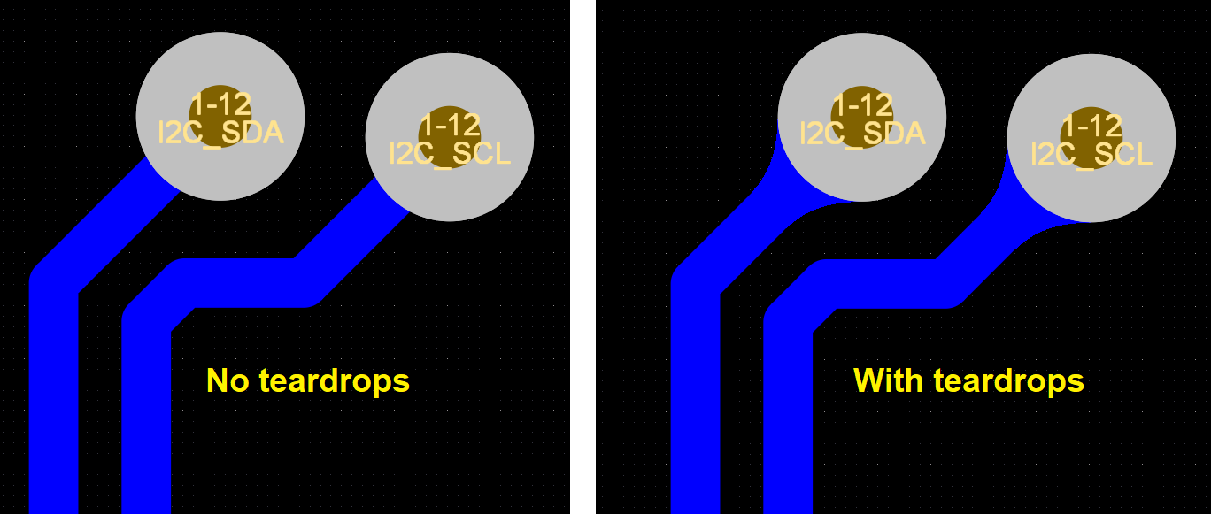
Solution - The simplest solution is to add teardrops to the design to provide some additional copper, although you might also need to increase the size of via pads to ensure there is enough copper to leave sufficient annular ring after drilling. Some fabrication houses will add this for you during an engineering review. Also do not forget that a fabrication house cannot read your mind: if you need the design to meet Class 2 or higher qualification standards, then you need to communicate this to the fabricator when you create your order.

Use teardrops to compensate for smaller via pads that may not meet Class 2 qualification.
Consistent Net Names But No Net Connection
Problem - Imagine for a moment: you try to bring up a board, but certain connections aren't getting signal or power. This is the result of an open circuit, but the design data does not show any unrouted nets. I have seen this occur when the same net name is defined in your schematics to define multiple connections, but one or more of the connections does not translate into the PCB layout.
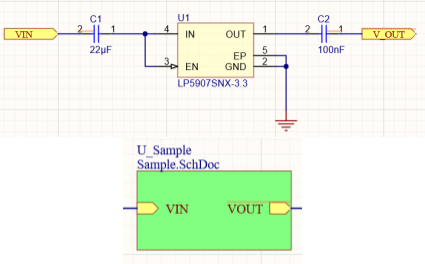
This would most commonly occur between input/output ports in a hierarchical design, where a single net connection is transferred across schematic sheets. Sometimes, there is an error where the net name is consistent, but the connection is not reflected in the PCB layout. I have also seen this occur when ports are not confined consistently across schematics, which will trigger a DRC error in your schematic editor.

Port naming error shown in a hierarchical project.
Solution - The solution here is attention to detail, consistent symbol usage, and consistent naming conventions. Similarly, ports in hierarchical designs must use consistent naming and I/O definition between sheets to ensure all net connections are transferred into the PCB layout.
Make sure to use the same symbol, net name, and punctuation across your hierarchical designs. In CAD systems, connections across schematic sheets require net names to be exact, right down to the punctuation or any special characters. It's also best to use a consistent symbol for the same net across a design, which mainly applies to power and ground ports (see below). This is useful for your own tracking of net connections across the design, and it will prevent simple errors like this from leaving open circuits in your PCB layout.

Wrong Connections Between Boards
Problem - Many electronic devices are built with more than one PCBA, and instead they rely on connectivity between multiple circuit boards. The connections are provided by board-to-board connectors, standardized or custom cables, or custom-designed wire harnesses. A problem can arise when the intended connections between two nets are not correct, leading to a bridge between two unintended signals. For example, you might end up with a short between power and ground, power and signal, two different signals, etc.
This can occur for a very simple reason: the pinout was translated incorrectly between the two boards. The result is an incorrect connection, which can be seen when manually examining the pin naming scheme across the mating connectors. An example is shown in the image below, where we see two net name mismatches on a pair of pin headers that will be connected with a ribbon cable.

It's best practice to use consistent net naming between the mating connectors on two boards in a multiboard assembly. However, if you have two different PCBs that must mate to each other, just naming the nets consistently does not allow your DRC system to verify a mistake was not made.
Solution - The solution lies in the capabilities of your CAD tools. Advanced CAD systems like Altium Designer provide a set of multiboard design features that can check for correct logical connectivity across two or more boards. This means you're less likely to miss a net name mismatch between two boards, and instead the mismatch can be caught by the DRC system. If you don't have these capabilities, you will always need to check and re-check the pinouts on the mating connectors to ensure no mistake was made.
Move Slow and Don't Break Things
In the past few years, I've noticed met many hardware founders and I've noticed they came from the software world. Too many hardware startups think they can apply the typical software startup roadmap and blitzscaling to their hardware company. In the hardware world, we have to be more conservative because there are very few simple fixes to prototypes that can eliminate defects. Don't be too eager and don't just straight into high volume; make sure every aspect of your prototype is thoroughly qualified and tested before you scale, and you'll be able to avoid many of the first pass perils I discussed above.
Large enterprises, small startups, and individual designers trust the complete set of PCB design features and world-class CAD tools in Altium Designer® to help them build advanced devices that push the limits of modern electronics. To implement collaboration in today’s cross-disciplinary environment, innovative companies are using the Altium 365™ platform to easily share design data and put projects into manufacturing.
We have only scratched the surface of what’s possible with Altium Designer on Altium 365. Start your free trial of Altium Designer + Altium 365 today.


