


CP2102 USB to UART Module PCB Design Project

At a Glance
See how to use the CP2102 in a new project for a USB to serial converter module. You can use the same steps to place this on a larger PCB.


Click here to jump to the viewer embed and browse this project
There is a group of products I work on that require boot and configuration over RS-232 or UART, and I like to boot prototypes by connecting them to my laptop. However, in order to access that interface, I have to send data and receive over a COM port. Unfortunately, my laptop only has USB ports, so I need to convert between the USB port and the UART interface. Normally I use a small interface converter module that can be purchased online.
The converters I’ve found online are pretty low quality and they tend to die from shock or overvoltage pretty easily. To provide some overvoltage protection, I’m going to show how to design a USB to UART bridge using the CP2102, a popular interface converter component for USB 2.0 lines. You can watch the full tutorial for this project in the following video.
You might be wondering, why not just place one of these circuits on prototypes directly, and then access the UART interface on your prototypes with a USB cable? This is a fair question. There are two reasons for this:
- Not all embedded products will support USB, but I’m struggling to remember an embedded product I’ve built that didn’t have a UART interface.
- Placing an extra USB port with a data converter chip on every single prototype adds extra work and takes up space. It’s simpler to just place a 2-pin header for the UART lines.
So with this in mind, let’s get to work on a small module for a CP2102 USB to UART converter.
Getting Started With the CP2102
The CP2102 from Silicon Labs is a compact interface converter module that bridges USB and UART interfaces. I like this component for systems that need to connect to USB because there are ready-made drivers for the chip that allow it to be accessed over a COM port through a terminal application (I use TeraTerm). This chip is one of many that is used in USB-to-serial converters that you’ll find on Amazon or Alibaba.
The CP2102 comes in a QFN-28 package and includes some useful features:
- Integrated +5V to +3V3 regulator to power lower voltage devices
- Programmable ROM for implementing product data
- Simple optional reset pin and circuit
- Integrated clock, eliminating the need for an external crystal
- Option to power with +3V3 input
- Data transfer via USB 2.0
There is also an optional bank of pins that act as indicators or control pins when used on the same board as a processor, such as a microcontroller. These pins can be controlled by GPIOs. We don’t need these for this module as the module will operate independently of any microcontroller.
Schematics
The design goals for this project are simple: the design will output its UART data, power, and ground to a pin header. The design will need to fit into a standard bank of USB ports. Finally, I’m going to add additional overvoltage protection on any data lines and the +5 V bus line to provide maximum overvoltage protection to the CP2102 and to the host device.
First, let’s look briefly at the application circuit for the CP2102 (page 15 of the datasheet).

The schematics will generally follow this application circuit with some additions to be discussed below. Because we are only using this module on the board without any other digital components, we don’t need to worry about additional power bus capacitance other than the discrete capacitors specified in the application diagram. After looking at other modules that use this and similar components, you’ll see the same type and number of capacitors.
TVS Diodes
In this application diagram, we see the typical recommendation for placement of TVS diodes on the USB lines. The part that they recommend is Littlefuse SP0503BAHT or equivalent. Initially, I placed a 0402 unidirectional TVS diode for this component. As I discuss below, this will just be a placeholder for now and it will get swapped in the final assembly.
We won’t be using any of the external transceiver circuitry or the reset pin in this iteration. Instead, we’ll just use the circuitry on the left side of the screen. I’ll also add TVS diodes to the UART Rx and Tx lines. The maximum voltage level that can be expected for this line is VDD - 0.8 V. with maximum VDD = 3.6 V, the maximum UART line voltage will be 2.4 V.

To provide maximum possible protection on the UART lines, we could place a TVS diode with a smaller breakdown threshold. The recommended TVS diode only protects up to 5.5 V, which is just under the overvoltage rating for I/Os on the CP2102. The risk of using a smaller TVS diode is that it will have lower clamp voltage and will not be able to withstand higher voltage ESD pulses.
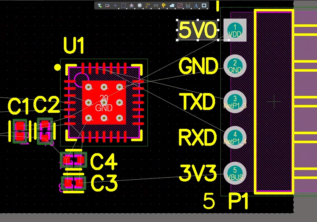
The finalized schematics are shown below. The device is simple and essentially follows the application circuit. I’ve taken the approach to use the +5V power coming into the module from the USB connector (VBUS net) and I’ve passed this to the regulator input on the CP2102. The +5V power and the output +3V3 power are both accessible on the pin header and can be used to power an external device up to the power limits in the USB 2.0 standard.

PCB Layout
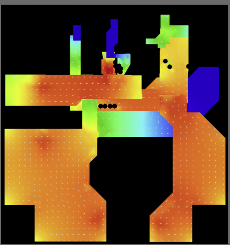
The PCB layout will be built on two layers with all components placed on the top layer. The PCB layout will be small enough that we don’t necessarily require high-speed routing of the USB lines, but we’ll implement it here as a simple example to show how it can be done in this type of board. This board is simple enough that it does not need to be placed on four layers and the USB routing requirements can be satisfied with coplanar differential routing.
The initial placement is covered in two sections; the USB connector and TVS diodes for the USB lines are placed on the left side of the board, and the pin header with diodes D4 and D5 are placed on the right side of the board. Placement in the left side of the PCB layout is shown below.

The initial placement on the pin header side is shown below. I used a right-angle pin header that hangs off the edge of the board so that the module would be low profile. This also allows standard flying leads or a 100 mil pitch cable to be used to connect to another board. Initially, the pinout was set so that the +5 V power (VBUS net) would route into the pin header at the top side, but this was later changed to the bottom side to simplify the routing.
The placement is simple on both edges of the board and the major point here is to keep the caps (C1-C4) close to their respective power pins. The placement of D4 and D5 will be between U1 and P1, but I’ll locate these once routing starts so that I can make sure the routing near them won’t get messy. The USB routing can now go straight into the connector (J1) with this placement. The next point is to calculate the USB trace width and spacing on this 2-layer board.
Based on cost minimization, the board should be set to the standard thickness of 62 mils. The back side will be ground pour, and the top side will use coplanar routing for the differential pair. The rest of L1 will have copper pour. I’ve used the default Dk setting of 4.8 in the stackup, which is very close to my selected fabrication house’s standard value for 2-layer PCBs. The impedance settings are shown below.

Here, we’re taking advantage of the spacing between the pairs and the distance to the copper pour on L1 to set the differential impedance to the target value. The width value was set based on the size of the pads on the CP2102 as I don’t want to neck-down the routing into the footprint for U1. With these settings, we can route the differential pairs into the connector and complete the layout.
The finalized PCB layout is shown below. There is extra length here that could be deleted if we want to miniaturize the module. Just using the measurement tool (Ctrl + M), I would estimate we could cut out about 400-500 mils of length just by grabbing the components in the right half of the board and moving them closer to the USB connector.

Currently, the size of this module is similar to other modules you can purchase online, so the above point is not critical. There are three other improvements that could be implemented in this project:
- Add small SMD indicator LEDs in parallel with the UART Rx and Tx lines so we have a visual indicator of data transfer
- Add reverse overvoltage protection on the 3V3 line; the same components used on the USB line could be used here
- Add a reset circuit with a small switch
I’m going to get a batch of these into production, and we’ll go through some testing to verify that the boards work correctly. As I’ll outline in another video and blog, I’m likely going to replace the diodes with TPD1E10B06DPYR in the assembly as these alternative diodes provide bidirectional protection and they are closer to the SP0503BAHT specs.
Follow this link to download a ZIP archive with the project source files. You can also use the download link in the above embed to access the source files.
Whenever you need to quickly create small modules and prepare them for manufacturing, use the 2D and 3D CAD tools in Altium. When you’ve finished your design, and you want to release files to your manufacturer, Altium makes it easy to collaborate and share your projects.

About Author
Related Resources
Related Technical Documentation
Table of Contents
Design to Release, Without the Friction
- Keep reviews tied to the right version
- Reduce handoff confusion and rework
- Spot sourcing and release risk earlier
- Work solo, share when needed
Get Started
Thank you, you are now subscribed to updates.

