


Designing for Tight Spaces: Top Mechanical Challenges

At a Glance
Mechanical engineers face thermal, spatial, and EMI hurdles in compact designs. Learn how ECAD-MCAD codesign helps solve them fast.


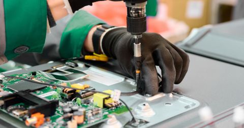
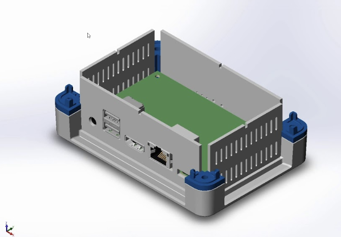
The defining trend in modern electronics is a paradox: devices must shrink in size while expanding in power and functionality; this relentless push for miniaturization, from handhelds to wearables, has fundamentally reshaped the role of the mechanical engineer. The days of designing a simple ‘box’ to house a PCB are gone. Today, the enclosure is an active, elaborate system that must provide structural integrity, manage heat, and shield from electronic noise, and the historical wall between mechanical (MCAD) and electrical (ECAD) design is no longer sustainable.
Key Takeaways
- Miniaturization has turned enclosures into active systems that must manage structure, heat, and EMI, making tight ECAD–MCAD collaboration essential rather than optional.
- Disconnected, file-based workflows (STEP/IDF handoffs) slow iteration, obscure design intent, and dramatically increase the cost of late-stage errors.
- Mechanical engineers face three core challenges in compact designs: precise 3D clearance management, effective thermal dissipation in high power density layouts, and robust EMI/RFI shielding.
- Thermal and electromagnetic issues escalate quickly in dense designs, where small layout or enclosure changes can have outsized impacts on reliability and compliance.
- Live, synchronized ECAD–MCAD integration enables earlier detection of mechanical, thermal, and EMI problems, reducing rework, prototype spins, and overall development risk.
The High Cost of a Disconnected Workflow
Before exploring the technical hurdles, it is essential to understand the procedural problem that exacerbates everything: the persistent disconnect between ECAD and MCAD workflows. For decades, collaboration has relied on exchanging static files like STEP or IDF. The electrical engineer finishes a design and exports a ‘snapshot’ for the mechanical engineer to import, check, and manually rebuild.
This process is fraught with issues:
- It discourages iteration. The workflow is so cumbersome that both sides hesitate to make small, iterative changes, leading to infrequent, monolithic updates.
- It creates ambiguity. Important design intent is lost in translation. A 3D component model in an MCAD tool lacks the critical context of whether it's a simple plastic connector or a metal-cased capacitor that could cause a short.
- It invites error. Version control becomes a nightmare of tracking file names, emails, and verbal instructions, making it easy for outdated information to persist in the design.
This friction has a staggering financial impact. A study by NASA found that if fixing a design error during the requirements phase costs 1x, fixing that same error during manufacturing costs 7-16x more. If it’s not caught until testing and integration, the cost explodes to 21-78x. With tight margins and fierce competition, these preventable errors, born from a disconnected workflow, can jeopardize an entire project.
The Gauntlet of Miniaturization: Core Mechanical Challenges
The theoretical costs of poor collaboration become painfully real when MEs confront the physical realities of compact design. Every decision is a negotiation between competing requirements, where a change made to solve one problem can easily create another.
Challenge 1: The Three-Dimensional Puzzle
The most immediate challenge is fitting everything into a shrinking physical volume; this spatial puzzle is a battle for every last millimeter.
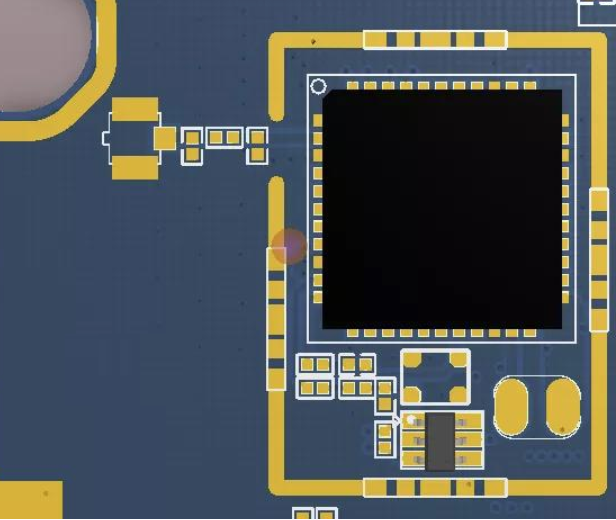
- Clearance Management: Mechanical engineers must prevent interferences down to the smallest detail - screw heads, cable bend radii, connector housings, even a solder fillet that might short against a conductive wall. Many prototypes fail simply because the case won’t close.
- Digital vs. Physical Reality: CAD models don’t show manufacturing deviations. Tolerance stack-up, warping, or shrinkage in molded parts can mean the difference between perfect assembly and costly tooling changes.
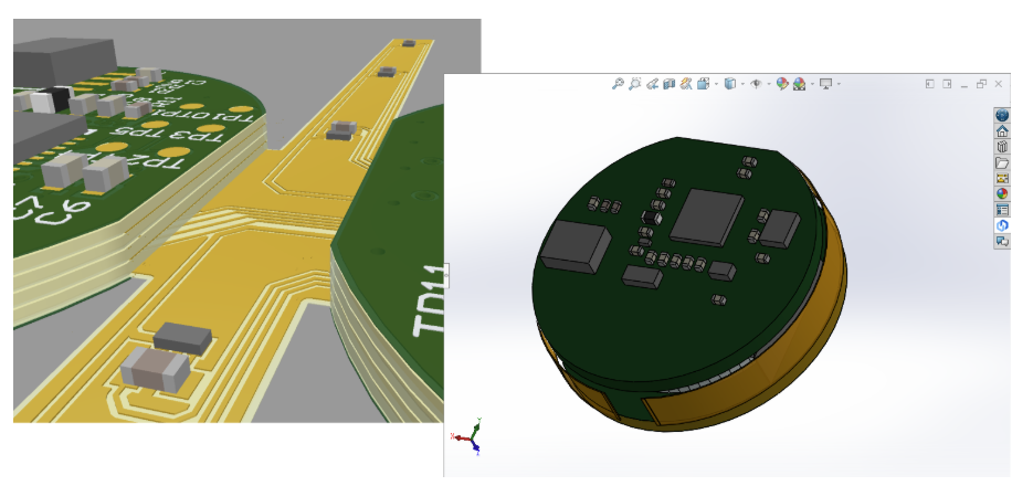
- Rigid-Flex Integration: Organic shapes and tighter layouts often require rigid-flex PCBs. While electrical engineers design the circuitry, MEs define folded geometry, bend limits, stiffener placement, and stress management for copper traces, key to long-term reliability.
Challenge 2: The Thermal Threat
As components become more powerful and densely packed, they generate a tremendous amount of heat in a very small space. For MEs, managing this thermal load is a critical factor in product reliability and safety. The rule of thumb is: for every 10°C increase in operating temperature, the reliability of electronic components is cut in half.
This challenge is rooted in physics. Higher power density means more heat is generated per unit volume, with less surface area available to dissipate it. The ME must design an effective thermal management system within the product's constraints; their toolkit includes:
- Passive Cooling: Designing the enclosure itself to act as a heat sink, using thermally conductive materials like aluminum and incorporating fins to increase surface area.
- Active Cooling: Strategically designing airflow paths with vents and integrating fans or blowers to force cool air over hot components.
- Simulation: To get around the need for thermal prototypes, CFD simulations can be used to predict hotspots and validate a cooling strategy.
Challenge 3: The Noise Within (EMI/RFI Shielding)
When electronic components are packed closely together, the electromagnetic fields they generate can interfere with one another, causing everything from poor signal quality to complete device malfunction. When the PCB layout is modified to address noise and there are still challenges with noise coupling, the ME may be asked to determine whether a PCB-mounted shield can be added to the design.
The core principle of shielding is the Faraday Cage, an unbroken conductive enclosure that blocks electromagnetic fields. However, a real-world product isn't a sealed box; it needs openings for ports, buttons, displays, and ventilation. Each aperture is a potential leak that compromises the shield, so the ME must employ a variety of strategies to create a functional shield, including:
- Using metals like aluminum for the enclosure or applying conductive paints to plastic housings.
- Using conductive gaskets to close the seams between enclosure parts, maintaining the electrical continuity of the Faraday Cage.
- Designing mounting points for small metal ‘cans’ that can be soldered directly over specific noisy components on the PCB.
Altium: A Modern Approach
These challenges - spatial, thermal, and electromagnetic - all point back to the same root cause: the friction and data loss inherent in a disconnected, file-based ECAD-MCAD workflow. The solution is to abandon the old model of exchanging static files and move to a live, synchronized, and truly collaborative environment.
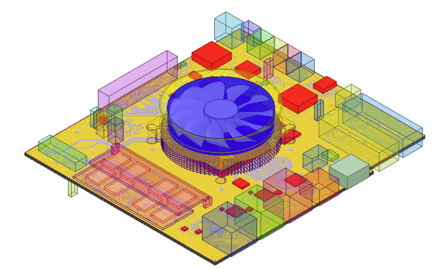
The best new environment is built on direct integration, where the ECAD and MCAD tools communicate in real-time through a shared platform like ECAD-MCAD codesign in Altium Develop. Instead of waiting for an IDF or STEP file, the ME can pull the live PCB design directly into their native MCAD environment. Note that this isn't a dumb solid; it’s a high-fidelity model complete with actual 3D copper traces, vias, and silkscreen decals; rich data that is transformative:
- For spatial challenges, the ME can now perform truly accurate clearance checks against the real copper geometry, not just a simplified component extrusion. They can define or modify the board outline, move mounting holes, or define keep-out areas, and push those changes directly to the EE as clear, actionable proposals.
- For thermal challenges, the ME can use the high-fidelity PCB model, with its accurate copper data, to run meaningful and realistic thermal and structural simulations (FEA/CFD) from the very beginning of the design process.
- For communication breakdowns, every push and pull is tracked with comments and a full version history, which creates a single source of truth and an unambiguous, auditable record of every decision, eliminating the risk of working from outdated information.
An integrated workflow eliminates the communication gaps that cause late-stage errors and costly prototype rework. Electromechanical issues can be found and fixed in minutes instead of weeks. Beyond speeding development, it reduces time spent managing files and tracking information, allowing engineers to focus on proactive co-design. This enables teams to confidently tackle more complex designs.
Whether you need to build reliable power electronics or advanced digital systems, Altium Develop unites every discipline into one collaborative force. Free from silos. Free from limits. It’s where engineers, designers, and innovators work as one to co-create without constraints. Experience Altium Develop today!
Frequently Asked Questions
Why isn’t exchanging STEP or IDF files enough for modern PCB and enclosure design?
Static file handoffs are slow and error-prone. They lose design intent, make version control difficult, and discourage iteration. In compact, high-power designs, these gaps often lead to late-stage mechanical clashes, thermal issues, or EMI problems that are expensive to fix.
What are the biggest mechanical challenges caused by electronics miniaturization?
Mechanical engineers typically struggle with three areas: fitting components and assemblies into extremely tight 3D spaces, dissipating heat from high power density electronics, and controlling EMI/RFI in enclosures that require openings for airflow and connectors.
How does ECAD–MCAD integration reduce rework and prototype spins?
Live, synchronized integration lets mechanical engineers work with accurate, high-fidelity PCB data (copper, vias, and real component geometry) so clearance, thermal, and EMI issues can be identified and resolved digitally instead of during physical prototyping.
When should mechanical engineers get involved in PCB design?
As early as possible. Early collaboration allows enclosure constraints, mounting, cooling strategies, and shielding requirements to inform PCB layout before designs are locked, preventing costly redesigns later.
What makes a modern ECAD–MCAD workflow different from traditional collaboration?
Modern workflows replace file exchanges with real-time co-design. Changes, comments, and revisions are tracked in a shared system, creating a single source of truth and eliminating confusion about which version of the design is current.

About Author
Related Resources
Related Technical Documentation
Table of Contents
- Key Takeaways
- The High Cost of a Disconnected Workflow
- The Gauntlet of Miniaturization: Core Mechanical Challenges
- Challenge 1: The Three-Dimensional Puzzle
- Challenge 2: The Thermal Threat
- Challenge 3: The Noise Within (EMI/RFI Shielding)
- Altium: A Modern Approach
- Frequently Asked Questions
- Why isn’t exchanging STEP or IDF files enough for modern PCB and enclosure design?
- What are the biggest mechanical challenges caused by electronics miniaturization?
- How does ECAD–MCAD integration reduce rework and prototype spins?
- When should mechanical engineers get involved in PCB design?
- What makes a modern ECAD–MCAD workflow different from traditional collaboration?
Design to Release, Without the Friction
- Keep reviews tied to the right version
- Reduce handoff confusion and rework
- Spot sourcing and release risk earlier
- Work solo, share when needed
Get Started
Thank you, you are now subscribed to updates.