
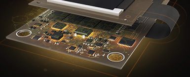


Flexible Circuit Designs with Large or Heavy Components
One of the primary benefits of using a flexible circuit versus a rigid PCB board or wire and cable is the savings in weight and space. Flexible materials are thin, extremely light weight, and allow you to package in 3D, bending and folding to make necessary connections, allowing you to shrink the overall package size or fit additional electronics in a similarly-sized unit. As an example, a very typical two-layer construction for a flexible circuit is .010”, including coverlay and can often be even thinner than that. But what happens when you have a larger, heavier component that is going to be assembled to this flexible circuit? Connectors can often outweigh the flexible materials and require special attention during assembly and installation.
Let me share a story. A two-layer flexible design required a large, heavy connector in the center of the flex and an FR4 stiffener was included for added support in that area, which is the recommended design practice. As it was being assembled, the engineer observed cracked traces and failures in this area. This was originally attributed to the FR4 not being thick enough to support the component. Because time was tight (isn’t it always?), a second FR4 stiffener was added to the other side of the flex as a short term fix to provide additional support before assembling the through-hole connector. This adjustment did not fully resolve the issue, but it did improve yield enough to be able to fulfill the prototype build.
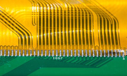
As this moved from prototype to pre-production volumes, the full design was reviewed for yield improvement opportunities. A few different things were done mechanically: the thickness of the FR4 stiffener was increased, and the thickness of the flexible materials was also increased to provide additional support. What was most interesting, is that it was also identified that in that component area, best design practices were not followed. The pads were not tear-dropped. The intersection of the trace and pad area is one of the highest stress areas of a flex design and it is always recommended to add the largest fillets possible to your flex designs. In this case, not only was the component putting stress on the pad to trace transition areas, those areas were already at high risk.
What are some of the things to consider to successfully navigate the challenge of a heavy component needed on a thin flexible circuit? One of the first decisions that needs to be made is whether to use a flexible circuit with a stiffener or a rigid-flex construction. There can be confusion with regard to the terminology of a rigidized flex when compared to a rigid-flex. To be clear, a rigidized flex is a flexible circuit with an FR4 stiffener added to provide support to component areas. This stiffener is purely a mechanical support. A rigid-flex, on the other hand, will typically have circuitry on the rigid layers and use plated through-holes to electrically connect the rigid and flex layers.
This decision should factor in the full scope of the flex and assembly, not just the larger heavier connector area. Often, with lower layer count flexible circuits, a flex design with added FR4 stiffener is a logical, lower cost alternative to a rigid-flex. But a rigid-flex construction should not be readily dismissed if there are multiple, higher density component areas, particularly on both sides of the board.
Once the decision is made to move forward with a rigidized flex, there are several things to take into consideration with the design. First, what is the shape and thickness of the stiffener? Typically, FR4 stiffeners are created by taking rigid board laminate and etching the copper on both sides, then drilling and routing the appropriate size and shape. Common FR4 stiffener thicknesses range from .003” (0.008mm) to 0.125” (3.18mm). The overall size of the stiffener should include a review of not only the size of the component being supported, but also how that stiffener might influence nearby bend and fold areas.
Once the stiffener is designed, a decision needs to be made as to how the stiffener will be bonded to the flex circuit. Will bonding the stiffener to the flex with a pressure-sensitive adhesive be sufficient or will the application require a thermal set adhesive to used? PSA’s are typically a lower-cost option, not requiring an additional lamination cycle by the fabricator.
We talk quite a bit about following good design practices for flexible circuit designs including tear dropping the pads, providing tie downs or rabbit ears for those pads, routing perpendicular to any bend and fold areas, keeping plated through-holes away from bending and folding areas, etc. As we saw from the example earlier, this is critical even if the area is going to be supported by a rigid stiffener. Bypassing these recommendations can prove to be a costly shortcut.
One last recommendation when using a rigid stiffener to support a heavy component on a flexible material is to be sure to add an entry in the fabrication notes to have epoxy applied at the flex and rigid interface to help reduce the stress on the traces in that area.
Don’t be nervous about using a larger, heavier component on a thin, lightweight flex circuit, just be sure to follow the best practices for design!
Have more questions? Call an expert at Altium or continue reading about flex and rigid-flex PCB assembly in Altium Designer®.
About Author
Related Resources
Related Technical Documentation
Altium is transforming the electronics industry so thoroughly that our web pages need a minute to catch up. For a short time, some information on this page may be outdated.
We appreciate your patience. It will be worth the wait!
Learn More
Thank you, you are now subscribed to updates.