



How to Design Boards That Work With the Process Not Against It

At a Glance
This article explores effective strategies for designing printed circuit boards (PCBs) that enhance collaboration with fabricators and streamline the manufacturing process. It highlights that many delays in PCB fabrication arise from inadequate documentation and unrealistic tolerance specifications rather than defects in manufacturing.


Most PCB fabrication delays are not caused by manufacturing defects. They originate in incomplete documentation, ambiguous tolerance callouts, and material specifications that do not align with the fabricator's standard process capabilities. Treating DFM as a checkbox at the end of the design cycle, rather than an integrated design activity, is the root cause of most first-build schedule slips.
The real engineering problem is that designers often release data packages optimized for electrical performance without accounting for the fabricator's process constraints. A design that passes all EDA rule checks can still be unbuildable, or buildable only with costly process exceptions, if the documentation does not communicate design intent clearly enough for the fabricator to make correct process decisions.
Key Takeaways
- Most PCB fabrication delays stem from documentation failures, not manufacturing defects. Incomplete fab notes, ambiguous tolerance callouts, and material specs that don't match the fabricator's standard process capabilities cause more first-build schedule slips than anything on the shop floor.
- Call out only functionally-driven tolerances explicitly. Specifying tight tolerances across every feature drives cost without improving the product. Impedance control, flex-rigid transitions, annular ring requirements on microvias, and hole positional tolerances deserve explicit callouts; everything else should default to standard process capability.
- Gerber files alone don't communicate design intent. A complete fabrication documentation package, covering controlled impedance targets, material requirements, stackup intent, and region-specific processing needs, eliminates days of back-and-forth that would otherwise delay the build.
- DFM review belongs in the workflow, not at the end of it. Any change affecting copper geometry, the stackup, or stencil apertures requires re-running DFM checks before release. Engaging the fabricator's DFM review early catches process-specific issues that EDA rule checks cannot flag.
Material Selection and Procurement Risk
Specifying a single laminate material by manufacturer and part number creates a procurement dependency. If your fabricator does not stock that specific material or run it regularly, you introduce procurement delays and process risk simultaneously.
The practical approach is to identify which material properties are non-negotiable for your design (loss requirements at your operating frequency, Tg for your thermal environment, CTE matching for reliability) and where you have flexibility. Giving your fabricator latitude on material selection, where performance requirements allow it, often results in better pricing and shorter lead times.
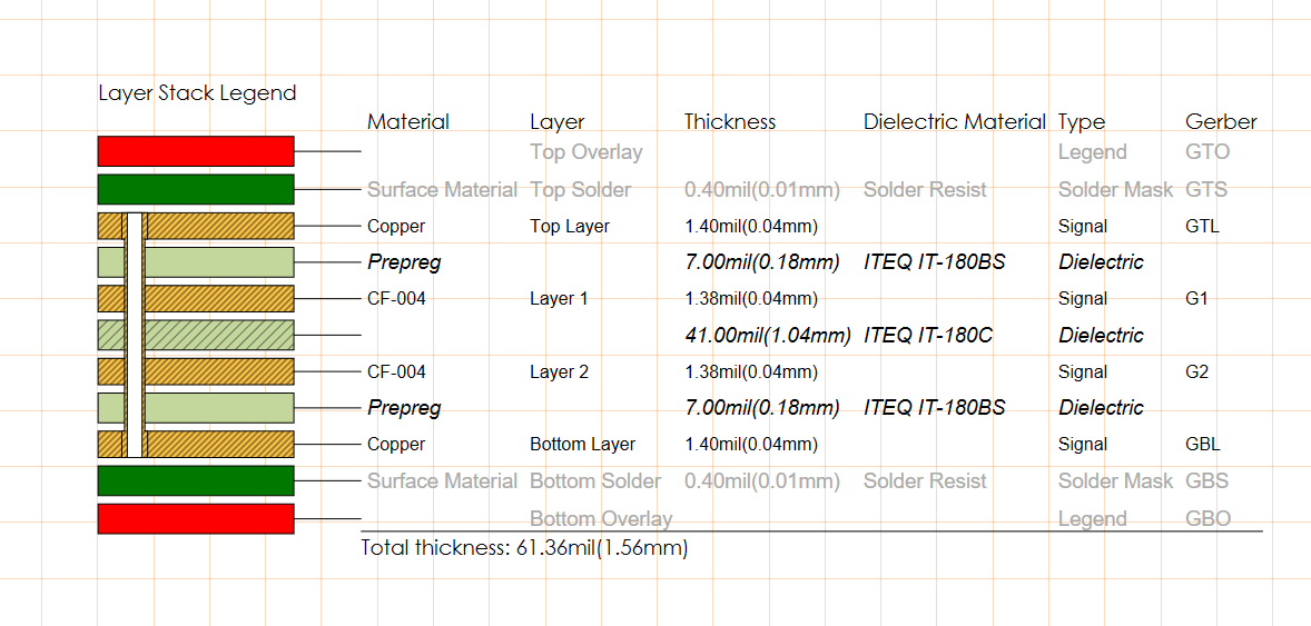
Stackup drawings can call out specific thicknesses and commercial material brands as shown in this image from Altium’s Draftsman.
Tolerance Callouts That Drive Cost
A fabrication drawing that specifies only "Build to IPC-6012 Class 2, newest revision" provides only basic guidance. Conversely, drawings that call out unnecessarily tight tolerances on every feature drive cost without improving the product.
The correct practice is to identify which tolerances are functionally driven and call those out explicitly. Impedance control on specific layers, registration between flex and rigid transitions, annular ring requirements on microvias: these deserve explicit tolerance callouts. Features that are not performance-sensitive should be left at standard process capability.
Impedance Control | Impedance Target by Layer |
Annular ring allowance |
|
Misregistration |
|
Trace width/spacing |
|
Hole size tolerance |
|
Hole positional tolerance |
|
Fabrication Documentation and Design Intent
Gerber files are one of the outputs that fabricators can use for building bare boards, but they are just one way to provide the documentation and requirements a fabrication house needs. Your fabricator has not been involved in your design decisions and cannot infer intent from copper geometry alone. The purpose of fabrication documentation is to communicate design intent clearly enough that the fabricator can make correct process decisions without guessing.
Effective fab notes should specify:
- Controlled impedance requirements with target values, tolerances, and reference layers
- Material requirements or acceptable substitutions with performance criteria
- Stackup intent, including dielectric thicknesses and copper weights
- Region-specific requirements, such as localized stiffeners, selective plating, or impedance coupon placement
- Features requiring special processing attention during drilling, lamination, or plating
A complete set of fab notes eliminates days of back-and-forth communication that would otherwise delay your build.
Late-Stage Design Changes and Verification
Design changes made after routing is complete can create DFM violations in dense or impedance-controlled areas, even when the changes appear minor. A moved trace may violate spacing rules relative to adjacent features. An added component may require a stencil modification that affects paste volume on neighboring pads.
Any change that affects copper geometry, the stackup, or the stencil aperture design requires re-running DFM checks before release. This is not optional for high-density or high-speed designs where margins are already tight. The cost of re-running verification is trivial compared to the cost of a fabrication hold or a board respin.
Integrating DFM Review Into the Design Release Process
DFM review should not be treated as a final gate before release. It belongs in your workflow alongside electrical verification as a standard design process step. Most fabricators will perform DFM review at no additional cost, particularly for established customers, and catching violations before release eliminates the most common source of build delays.
The fabricator's DFM review catches process-specific issues that your EDA tool's design rule check cannot flag:
- Panel utilization problems that affect pricing or delivery
- Drill aspect ratio limits for their specific equipment
- Registration concerns with their lamination process
- Material-specific processing constraints affecting layer-to-layer alignment
- Copper balance issues that cause warpage during lamination
Engaging this review early and treating the feedback as actionable design input reduces cycle time and improves first-pass yield.
Move From Design to Release With Less Friction
Getting fabrication documentation right is one part of a reliable release process. The other is having a workflow that keeps your design, your review, and your outputs connected from the first schematic through the final data package.
Altium Develop is built for hardware designers and small teams who want that clarity without added overhead. It gives you Altium-grade PCB design capabilities alongside a cleaner path from active design to review to release. No forced process change. No enterprise complexity you didn't ask for.
Get started with Altium Develop →
Frequently Asked Questions
What is the difference between DRC and DFM in PCB design?
A design rule check (DRC) verifies whether a layout meets the rules you defined in your EDA tool (clearances, trace widths, minimum annular rings). DFM goes further: it checks whether the design can be built reliably within a specific fabricator's real process capabilities, including drill aspect ratio limits, copper balance for lamination, panel utilization, and registration tolerances. A board can pass all DRC checks and still trigger a fabrication hold if the documentation doesn't align with how the fab actually runs their process.
What should PCB fabrication notes include?
Effective fabrication notes should cover:
- Controlled impedance requirements with target values, tolerances, and reference layers
- Material requirements or acceptable substitutions with the performance criteria that drive them
- Stackup intent including dielectric thicknesses and copper weights
- Region-specific requirements such as selective plating or stiffener placement
- Any features requiring special attention during drilling, lamination, or plating
Gerber files communicate copper geometry, fab notes communicate design intent.
When should DFM checks be run during PCB design?
DFM checks should run alongside electrical verification throughout the design process, not only before release. Late checks can lead to internal engineering change orders, board respins, delays, and added cost. Any change that affects copper geometry, the stackup, or stencil apertures requires a re-run before the data package is released, even when the change appears minor.
Does specifying tight tolerances on every feature improve PCB quality?
No. Calling out unnecessarily tight tolerances on features that are not performance-sensitive drives fabrication cost without improving the product. Tight tolerances require process exceptions, additional setups or manual steps, that add cost and extend lead time. The correct practice is to identify which tolerances are functionally driven and call those out explicitly, leaving everything else at the fabricator's standard process capability.

About Author
Related Technical Documentation
Table of Contents
Design to Release, Without the Friction
- Keep reviews tied to the right version
- Reduce handoff confusion and rework
- Spot sourcing and release risk earlier
- Work solo, share when needed
Get Started
Thank you, you are now subscribed to updates.