


Your Guide to Gerber File Extensions in PCB Design

At a Glance
Gerber files come with multiple extensions but in only two common file formats. You can learn more about Gerber file extensions in this article.


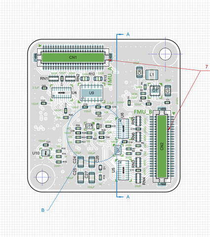
If you’ve ever used an external Gerber file viewer, or you’ve used some PCB design applications with a built-in Gerber viewer, you know there are different formats and file extensions for Gerber files. Some applications can very nicely reproduce the look and feel of a PCB layout with just a few active layers, such as the Gerber image I’ve shown above from one of our example press-fit connector layouts. The key to building and using these Gerber viewer applications is to understand the various Gerber file extensions and Gerber file formats.
What might seem like black magic to new designers is secretly intuitive, and it’s not as if one Gerber file extension is objectively “better” than another. If you’ve ever wanted to decode Gerber file extensions and formats, keep reading to learn more.
Gerber File Extensions vs. Gerber File Formats
Gerber files are the de facto industry standard format for encoding a PCB layout data into a format that is usable by vector photoplotters. We’ve discussed what is a Gerber file and the various Gerber formats in other articles on this blog, but we have yet to really dig into the various file extensions for each format. Experienced designers and fabricators have probably decoded the various Gerber file extensions, so this is focused more on newer designers.
To briefly review, what are the standard Gerber file formats, and what do they encode? The two Gerber file formats are the RS-274-X format (released in 1998) and the newer X2 format (released in 2014). These supersede the older RS-274-D format, which is no longer supported by its developer UCAMCO. Both file formats are ASCII human-readable files that can have any extension, and they can be read in a text editor just like other ASCII files.
- RS-274-X format: A 2D vector image of a specific layer in a PCB layer stackup; this file format includes aperture definitions, XY coordinate locations for draw and flash commands, unit data, special polygon fill commands, and other information needed for PCB fabrication.
- X2 format: Upgrades on RS-274-X format to include information on layer location, pads and vias, controlled impedance requirements, and other attributes. Upon the 2014 release, UCAMCO declared the earlier RS-274-D standard “technically obsolete” in favor of RS-274-X and X2 because aperture definitions in RS-274-D are not standardized.
- X3 format: The X3 format integrates fabrication, assembly, and component placement information into the Gerber file exports, similar to IPC-2581 but with multiple output files. Unlike earlier formats (e.g., RS-274X/X2), X3 incorporates detailed metadata such as reference designators and part numbers, consolidates pick-and-place data, and eliminates the need for separate BOM and placement files.
Aside from the X3 format, the earlier formats also require separate drill files, a BOM, centroid files, netlists, and a few other fab & assembly drawing files give your manufacturer everything they need to understand your board. To read more about the pros and cons of each format, read this older (but still relevant) blog post from Ben Jordan.
Regarding file extensions specifically, there is no specific extension for Gerber files defined in the de-facto standard or in CAM editors for viewing Gerber files. To see where the file extensions come into play, it helps to look briefly at an example with a finished PCB layout. I’ll show the set of Gerbers I’ve generated for a product I’m designing, and we’ll be able to see what the Gerber file extensions mean by looking at the Gerber file extensions under both standards.
CAD-Specific Gerber File Extensions
The image below shows a set of Gerbers (either RS-274-X or X2) for an example 2-layer PCB. From this list of files, we can see that they all have different extensions. The extension has the general format “GXY”, where X and Y refer to a specific function and/or layer assignment for the particular file. Under the RS-274-X and X2 standards, there are no attributes attached to each file, and the correspondence of each file to a specific layer in the PCB occurs through standardization of the file extensions.

When these Gerbers are imported into a CAM tool, the application can usually infer the function of each layer simply by looking at the extension. I say “usually” because not all CAM tools will do this automatically. The data in these files is all ASCII data, so any number of applications can read that data and use it to generate 2D vector images of each layer. If the Gerber viewer/editor application you’re using doesn’t understand the Gerber format extension and can’t determine the location in the layer stack, then it will cue up the layers out of order (usually in alphabetical order), and you will have to rearrange these manually.
.GBR File Extensions
The RS-274-X and X2 export can also be created with .GBR file extensions, where a file will be created for each and every layer in the PCB stackup, including mechanical layers. Files will also get generated for drill holes in the design, including for plated and unplated through-holes. If .GBR extensions are used, the generator utility will name all the files with the layer name from your CAD application and assign a .GBR file extension.
The image below shows the same set of Gerber files for the example 2-layer PCB, but exported with the .GBR extension.

In the above image, I’ve outlined the two signal layers in this simple board; there are no plane layers. The rest of the layers contain a set of data needed for fabrication and assembly. In this case, because a uniform file extension is used, most Gerber viewer applications will not be able to automatically assign each file to a specific layer in the PCB stackup, so the user will need to assign these manually.
Less Common Gerber File Extensions: .PHO and .ART
Technically, Gerber files could come with any file extension. I’ve received Gerbers as part of projects where the client’s engineer didn’t use the extensions shown above. The two less common file extensions I have received are:
- .PHO files (referring to photoplot, exported from PADS)
- .ART files (referring to artwork)
- No file extension
Note that less common extensions could come from naming conventions in specific CAD applications.
These files can be in either RS-274-X or X2 file formats, but they take the same approach as the .GBR file extension (one extension for all files, file names correspond to layer names). If this approach is used with RS-274-X files, then the same drawback applies: a CAM tool or Gerber viewer might not be able to automatically assign layer functions to these files unless the files are appropriately named. However, if X2 files are used, a CAM editor should be able to automatically assign each file to a specific layer because that information is encoded into each file.
Which Gerber File Extensions and Gerber Format Should You Use?
Truthfully, whenever I need to send in a design for fabrication, and the fabricator specifically asks for Gerbers, I simply create Gerber file extensions in X2 format and I create an ODB++ export. Giving them the option to use either the Gerber export of the ODB++ export eliminates a bit of waiting and some back-and-forth emails. I also send in a netlist, NC drill file, BOM, pick-and-place data, a set of fab & assembly drawings, and a STEP model of the board. If you send them everything and you keep it clearly organized in different folders, the fabricator will be able to choose exactly what they need and they can get the board into production quickly.
When you need to share your Gerber files and other fabrication data with your manufacturer or other designers, the easiest way is to use Altium. Using the Project Release feature, all the fabrication files you’ve generated can be easily shared with your manufacturer. Your manufacturer can then access shared files directly through Altium or through their web browser.
No matter which Gerber file extensions you prefer or what your fabricator demands, you can quickly generate a set of standardized fabrication files using the PCB design and manufacturing tools in Altium. The Output Job feature automates manufacturing file generation and ensures your documentation is error-free.
When you’ve finished your design, and you want to release files to your manufacturer, Altium makes it easy to collaborate and share your projects. We have only scratched the surface of what is possible to do with Altium. You can check the solution page for a more in-depth feature description or one of the On-Demand Webinars.

About Author
Related Resources
Related Technical Documentation
Table of Contents
Design to Release, Without the Friction
- Keep reviews tied to the right version
- Reduce handoff confusion and rework
- Spot sourcing and release risk earlier
- Work solo, share when needed
Get Started
Thank you, you are now subscribed to updates.

