Implementing Complex Pad Shapes

Component pads are not always simply round or rectangular shapes. Analog, high-power, or RF components often require geometrically complex or irregular shaped pads. This paper details an easy and efficient solution for when a user is confronted with having to quickly implement complex pad shapes that must meet the manufacturer’s layout requirements without resulting in DRC violations or manufacturing errors.
INTRODUCTION
Most component package types have consistent and straightforward rectangular or round pad shapes. Creating footprints for such packages, either manually or using an automated IPC footprint generator, is a simple process. However, occasionally component packages require complex pad design software shapes that can result in significant manual effort as well as additional time spent to get it just right.
For example, LED lighting components can require uniquely shaped heat dissipating pads that include multiple inverse curves. Such curves are impossible to implement by combining multiple standard round/rectangular pads or by manually placing fills or solid regions. However, an often overlooked method exists whereby if the outline of the required shape can be placed (or imported) as a series of tracks and arcs forming a closed outline, then the outline itself can be easily converted within the PCB Library Editor to a precisely-shaped solid region defining the pad. Furthermore, solder and paste mask can be automatically controlled by DRC rules through a property setting of the region object.
To better understand this method, the entire process can be explored by creating a footprint for a Bourns SRR5028 series shielded SMD power inductor as described below. To get started, a datasheet for this example can be obtained from the manufacturer’s website at http://www.bourns.com/docs/Product-Datasheets/SRR5028.pdffor part number SRR5028-101Y. Each pad device of this two-pin device includes an inverse curve with a 2.2 mm radius.
DEFINING PAD SHAPE OUTLINES
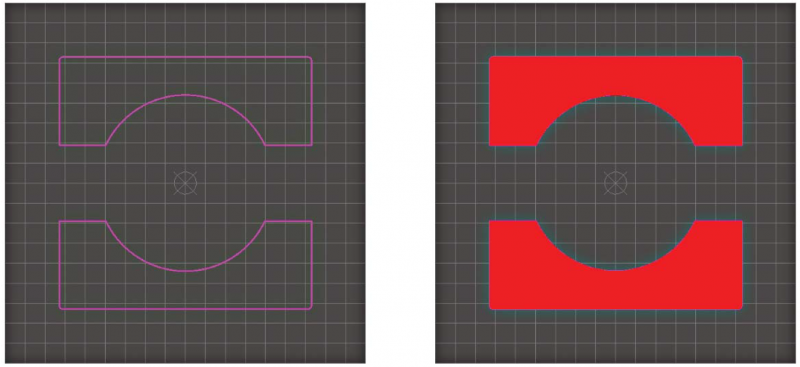
In the recommended layout section of the SRR5028 series datasheet, the key dimensions of the component drill hole pads are illustrated relative to the component origin. Within the PCB Library Editor, six lines and one arc are placed on a mechanical layer to capture these critical dimensions of each pad relative to the component’s origin (see Figure 1). The precise size and placement of these lines and arcs are then verified to be exactly in accordance with the manufacturer’s dimensions as shown in the datasheet. Setting the snap grid to 0.05 mm within the PCB Library Editor ensures the manufacturer’s dimensions can be precisely replicated.

Figure 1. Creation of mechanical outlines (right) from manufacturer’s datasheet (left).
Now that the critical dimensions of the component pads have been placed and verified, any extraneous lines or arc segments can be sliced, resized or removed altogether so that the end result is just two closed outlines on a mechanical layer, where each represents a pad shape. In this example, the closed outlines were manually created and verified. Alternatively, you can import complex pad shape outlines from DXF/DWG format if such data happen to exist and are more practical to use.
CREATING COPPER REGIONS FROM PAD SHAPE OUTLINES
With each components pad shape outline precisely placed and sized, they are now ready to be converted from lines and arcs on a mechanical layer to solid regions on the top copper layer. To do so, just select one outline, then make Top Copper the active layer, and use the PCB Library Editor Tools > Convert > Create Region from Selected Primitives command to create the actual solid region in the exact shape of the initially selected pad shape outline. The outside edges of the solid region are determined by the midpoint of the track and arc objects of the closed shape. Consequently, the dimensions of the solid region match those of the original schematic capture pad shape outline, as seen in Figure 2.

Figure 2. Conversion of pad shape outlines (left) to copper regions (right).
ADDING PAD DESIGNATION, SOLDER MASK, AND PASTE MASK
The inverse curve of each pad has been defined by quickly converting the outline of each pad shape. Note that it is not possible to implement such curves when manually placing a solid region object from the Place menu. At this point, just a couple of steps remains to complete the footprint. However, the most critical aspect of implementing these irregular pad shapes has now been addressed.
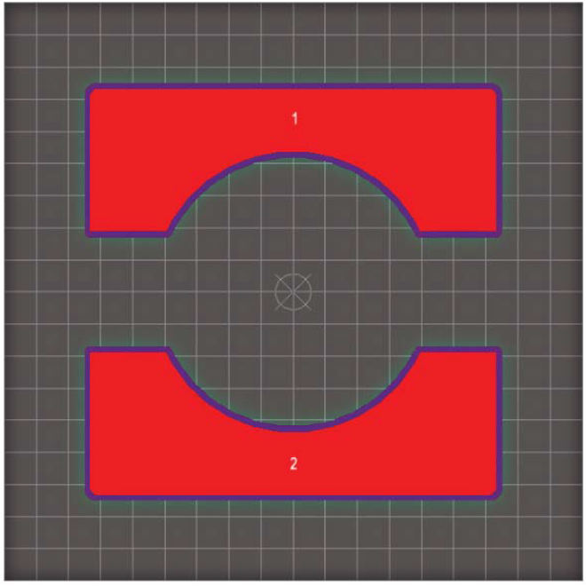
For each solid region to function as an actual component pad, a pad object must be placed directly within each solid area. In this example, two 1.0mm by 0.75mm rectangular pad objects designated 1 and 2 have been placed on the top and solid bottom regions respectively (Figure 3). These solid regions will now have electrical function as a regular component pad file.

Figure 3. Completed footprint including pad designations, solder mask, and paste mask.
Finally, to achieve a solder mask clearance as well as paste mask, the properties of both solid regions must be modified. This can easily be accomplished by selecting both solid regions and using the PCB Layout LIB Inspector to change both the Solder Mask Expansion Mode and Paste Mask Expansion Mode from None to From Rule. Just like any other pad object, these modified solid regions now fully function as pad objects from an electrical, fabrication, and assembly standpoint. The resulting footprint for the SRR5028-101Y component is now complete.
CONCLUSION
Occasionally some components will require geometrically complex or irregular shaped pads as per manufacturer’s recommended layout. Always remember that an easy and efficient solution exists to implement complex pad shapes quickly. By creating or importing a precise outline of the complex pad shape using tracks and arcs, the result can be converted to a solid region object. Combining each unique solid region with an appropriately designated pad object will enable each entire region to function electrically as an actual pad. Solder and paste mask attributes can then easily be set within each region for fabrication and assembly purposes.


