


How Electrical Engineers Use In-Mold Electronics to Integrate Circuits Directly Into Functional Surfaces

At a Glance
Discover how electrical engineers use In-Mold Electronics (IME) to embed circuits into 3D surfaces, enabling sleek, durable, and space-saving smart interfaces.


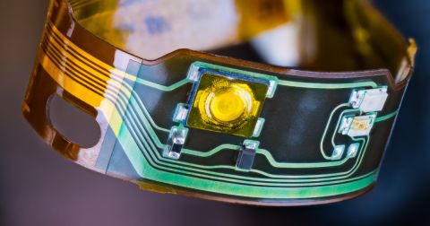
A dashboard control that appears as part of the surface itself, with no visible buttons or bezels, offers a sleek and intuitive user experience. This functionality is made possible by injection molded structural electronics (IMSE), a technology that embeds circuits directly into molded plastic rather than placing them on rigid PCBs. IMSE is reshaping how engineers integrate electronics into products by turning everyday surfaces into intelligent, functional interfaces.
The Problem with Traditional Interfaces
Electronic interfaces have long relied on a familiar formula: rigid circuit boards packed with components, tied to mechanical controls like buttons or switches, and encased within a protective housing. While functional, this legacy design creates significant drawbacks:
- Design Constraints: Cutouts, bezels, and mounting hardware restrict form factor innovation and industrial design flexibility.
- Reliability Issues: Every mechanical junction introduces a point of failure: wear, debris, or misalignment can lead to malfunction.
- Manufacturing Complexity: Building these interfaces demands multiple steps, specialized components, and costly assembly time.
- Bulky Form Factor: Discrete PCBs, controls, and enclosures eat up space and increase weight, factors that matter in automotive and wearable design.
- Environmental Vulnerability: Gaps and seams leave systems vulnerable to dust, moisture, and other contaminants.
The IME Revolution
In-Mold Electronics (IME) redefines how engineers embed circuitry into physical products. Instead of mounting electronic components on separate boards, IME prints circuits directly onto a flat thermoplastic film. This film is then thermoformed into a three-dimensional shape and encapsulated in injection-molded plastic. The outcome: a seamless, integrated structure where the electronics and physical form are one and the same.
The standard IME process includes:
- Printing: Conductive, resistive, and dielectric inks are screen-printed onto a thermoplastic substrate.
- Component Placement: Surface-mount components attach to the film using conductive adhesives.
- Thermoforming: Heat and pressure shape the printed film into the final 3D contour.
- Injection Molding: Molded plastic backs the film, creating a rigid, unified component.
This workflow introduces a range of practical advantages:
- Greater Design Flexibility: Engineers can integrate functionality into curved or contoured surfaces with ease.
- Part Consolidation: Dozens of discrete parts consolidate into a single structure.
- Enhanced Durability: Seamless construction removes potential failure points like buttons and connectors.
- Weight Reduction: By eliminating housings, PCBs, and hardware, total component weight drops by 40–70%.
- Manufacturing Efficiency: Simplified assemblies and reduced part counts lead to faster production cycles.
Research by IDTechEx reports that IME can cut part counts by up to 90% and lower interface manufacturing costs by 20–30%—a game changer for high-volume, feature-rich designs.
Real-World Success Stories
Automotive: Ford’s Mustang Mach-E Center Console
Ford’s electric Mustang Mach-E features an innovative center console with integrated controls manufactured using IME technology.
The design eliminated 50% of dashboard wiring and reduced assembly time by over 30% compared to traditional approaches.
The console integrates capacitive touch sensors, LED indicators, and haptic feedback elements into a single molded component, eliminating discrete parts that would have been required in a traditional design.
Consumer Electronics: Whirlpool’s Smart Appliance Controls
Whirlpool’s premium appliance line features IME control panels that have transformed both aesthetics and functionality. Their dishwasher control panel integrates 15 touch-sensitive controls, status indicators, and a display window into a single, seamless surface that can be wiped clean.
Buyers appreciate appliances that are both beautiful and easy to clean. IME allows manufacturing companies like Whirlpool to eliminate the crevices where dirt and moisture collect in traditional button interfaces.
The IME panels have proven 300% more resistant to cleaning chemicals than mechanical button arrays and have reduced warranty claims related to control failures by 45%.
Medical: Philips Portable Ultrasound Interface
Philips Healthcare’s latest portable ultrasound device features an IME control surface that has revolutionized both usability and infection control. The seamless interface eliminates crevices where contaminants can hide, allowing for complete disinfection between patients.
IME has allowed manufacturers to create interfaces that can withstand hospital-grade disinfectants while maintaining perfect functionality.
The Engineering Process: From Concept to Production
To understand how engineers apply injection molded electronics in smart surfaces, consider the development of an automotive climate control panel, beginning at concept and continuing through full-scale production.
1. Design Conceptualization
IME design doesn’t begin with schematics. It starts with physical form and interaction. Electrical engineers and industrial designers work together from the outset to define:
- The three-dimensional surface geometry
- User interaction points and feedback mechanisms
- Environmental tolerances such as temperature range, UV exposure, and chemical resistance
- Mechanical performance requirements including actuation force and impact durability
2. Material Selection
Every IME application hinges on material compatibility. Engineers evaluate:
- Base Film: Typically PET or PC, capable of withstanding thermoforming and injection molding conditions
- Conductive Inks: Often silver-based for conductivity, with carbon-based options used in cost-sensitive designs
- Dielectric Layers: Provide electrical isolation while maintaining flexibility and durability
- Injection Molding Resin: Typically PC, ABS, or PC/ABS blends engineered for adhesion to the printed film
Each material must hold its properties through the forming and molding processes without delaminating or losing functionality.
3. Circuit Design with Deformation in Mind
Printed electronics in IME must survive stretching and shaping during thermoforming. Engineers ensure reliability by:
- Designing circuits with elongation zones that can stretch without breaking
- Avoiding component placement in areas of high deformation
- Using stretchable circuit patterns (serpentine traces) in areas that will undergo significant forming
- Simulating the deformation process to predict stress points
4. Prototyping and Validation
IME prototyping typically follows a staged approach:
- Electrical Validation: Testing circuit functionality on flat films before forming
- Forming Trials: Testing the formability of printed circuits without components
- Functional Prototypes: Complete assemblies with components, tested for electrical performance after forming
- Injection Molding Trials: Validating that circuits and components survive the injection process
- Environmental Testing: Subjecting prototypes to temperature cycling, humidity, UV exposure, and chemical resistance tests
5. Production Engineering
Scaling IME requires fine-tuned process control:
- Screen Printing Optimization: Ensuring consistent ink deposition across production runs
- Component Placement Precision: Developing fixtures and processes for accurate, repeatable component attachment
- Forming Parameters: Defining precise temperature, pressure, and timing for thermoforming
- Injection Molding Setup: Optimizing gate locations, pressures, and temperatures to prevent damage to circuits
Overcoming IME Design Challenges
Injection molded electronics open new possibilities for product design, but they also introduce complex engineering problems that traditional PCB workflows don't address. Engineers must develop new strategies to ensure performance and manufacturability.
1. Elongation and Trace Reliability: When circuits undergo thermoforming, printed traces stretch along with the substrate. Maintaining electrical continuity under these stresses requires intentional design.
-
Serpentine Routing: Engineers use curved or zig-zag trace paths that can elongate without snapping.
-
Variable Ink Thickness: Thinner ink layers in deformation zones allow for controlled stretching without cracking.
-
Deformation-Aware Layout: Routing traces away from regions of peak stress minimizes failure risks.
2. Surface-Mount Component Integrity: Surface-mount devices must survive both forming and injection molding without detachment or thermal degradation.
-
Component Qualification: Only use parts rated for thermoforming and molding temperature profiles.
-
Thermally Safe Placement: Place sensitive components away from high-deformation zones.
-
Encapsulation: Shield vulnerable components during molding using protective overmolds or inserts.
3. Testing and Quality Control: IME requires alternative approaches to traditional PCB testing and inspection.
-
Functional Testing Fixtures: Custom jigs tailored to the 3D shape validate circuit performance post-forming.
-
3D Optical Scanning: Engineers verify circuit continuity and trace geometry with high-resolution surface inspection tools.
-
Alternative In-Circuit Techniques: Traditional test probes give way to flexible test interfaces or embedded self-diagnostic features.
What’s Next for In-Mold Electronics
IME technology continues to accelerate, and the next generation of innovations promises to expand its utility even further. As materials science, printed electronics, and additive manufacturing converge, several major developments are gaining traction:
Strechable Electronic
Researchers are advancing IME to support circuits that stretch far beyond traditional thermoformed limits. These elastic systems can elongate by 100% or more, enabling reliable integration into surfaces that undergo repeated flexing or expansion such as airbag covers, soft robotics, or medical wearables.
Printed and Embedded Sensors
Upcoming IME platforms will embed sensing directly into molded surfaces, eliminating the need for external sensor modules. Printed sensors will support:
-
Force-responsive interfaces using pressure sensors
-
Temperature monitoring in confined or sealed environments
-
Strain detection for predictive maintenance and structural health tracking
-
Gas detection for onboard air quality or industrial safety systems
Biodegradable and Sustanable Materials
Sustainability is emerging as a priority in advanced manufacturing, and IME is evolving accordingly. Ongoing efforts focus on:
-
Biodegradable substrates, such as cellulose-based films
-
Water-based conductive inks, offering reduced environmental impact
-
Recyclable molding polymers, suitable for automotive and consumer electronics
Design Software for IME Manufacturing Workflows
Creating high-performance injection molded electronics demands specialized software that supports the unique intersection of printed electronics, mechanical design, and scalable manufacturing.
Altium’s Integrated Tools for IME Development
Altium offers a suite of capabilities tailored to the specific needs of IME product development. These tools help engineers manage the complexities of designing circuits that will undergo thermoforming, molding, and environmental stress.
Key IME-supporting features include:
-
Material-Specific Design Rules: Enforce constraints based on the electrical and thermal properties of inks, substrates, and molding resins.
-
Printed Electronics Layer Stackups: Define non-traditional PCB structures within the Layer Stack Manager, optimized for printed electronics.
-
MCAD Compatibility: Seamlessly import 3D surface models from MCAD platforms to align electronic design with the final molded form.
-
Manufacturing Outputs: Generate custom files for screen printing, component placement, and forming operations, all from within a single environment.
By streamlining collaboration between ECAD and MCAD domains, Altium allows engineers to design smart surfaces with fewer iterations and faster turnaround. These tools accelerate the transition from concept to production for IME interfaces.
To start designing your own IME products, start the Layer Stack Manager in the PCB layout environment in Altium, then select the 3-line icon in the upper right.

You'll see multiple options for PCB types, such as Printed Electronics, Rigid-Flex, and others. For this workflow, select Printed Electronics. Once selected, your PCB stackup will be permanently updated to reflect this type, allowing you to define dielectric materials between conductive layers.
Altium's native support for printed electronics provides a design environment that understands the electrical relationships between sequential print runs. You can manually define insulating areas using dielectric materials or allow the system to generate them automatically at trace crossover points.
These conductive materials, such as copper, are printed onto flexible substrates, enabling the creation of bendable electronic circuits.
Complementary Tools in the IME Workflow
While Altium handles the electrical design aspects, a complete IME workflow typically includes:
- Mechanical CAD: Tools like SOLIDWORKS or Creo for designing the 3D form
- Forming Simulation: Software like Moldex3D or Polyflow to simulate the thermoforming process
- Injection Molding Simulation: Tools to predict how the injection process will affect the formed circuit
What IME Means for the Future of Product Design
In-Mold Electronics represents a fundamental shift in how we think about electronic interfaces. By integrating circuits directly into functional surfaces, IME eliminates the artificial boundary between electronics and structure, creating products that are more elegant, durable, and efficient.
For electrical engineers, IME requires a new mindset, one that considers electrical, mechanical, and manufacturing factors simultaneously from the earliest design stages. Tools like Altium are evolving to support this integrated approach, enabling engineers to realize the full potential of this transformative technology.
As IME continues to mature, we can expect to see it expand beyond user interfaces into structural electronics, where entire products become smart, responsive systems rather than passive housings for electronic components.
The future belongs to engineers who can think beyond the circuit board, who can envision electronics not as components to be housed, but as integral elements of the products they create.
Explore how Altium supports printed electronics and enables the integration of electrical circuits with three-dimensional mechanical parts.

About Author
Related Resources
Related Technical Documentation
Table of Contents
Design to Release, Without the Friction
- Keep reviews tied to the right version
- Reduce handoff confusion and rework
- Spot sourcing and release risk earlier
- Work solo, share when needed
Get Started
Thank you, you are now subscribed to updates.