


Printed Electronics: A Technology of the Past and Future

At a Glance
Discover how printed electronics is transforming industries with flexible, lightweight circuits. Explore materials, manufacturing, and design innovations in PE.


Printed electronics (PE) is a rapidly growing interconnect technology. While it has its roots in flexible printed keyboards for appliances and early printed circuits from WWII, today's advancements in materials, manufacturing, and design tools are pushing its capabilities far beyond its origins.
Printed Electronics - Applications
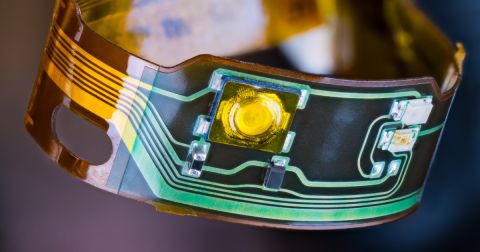
The most exciting aspect of PE is the expanding range of applications and markets. PE is being widely adopted across industries, from medical sensors to automotive interiors.
Some well-established applications include printed RFID tags, flexible glucose sensors, and printed batteries, while emerging innovations, such as in-mold electronics (IME) and printed millimeter-wave antennas, are opening up new possibilities.
Printed electronics have now also expanded into:
- 3D-Printed Functional Devices – Companies are developing systems that integrate 3D printing with PE, enabling interactive electronics, smart toys, and programmable circuits.
- Flexible & Wearable Electronics – The medical and fitness industries now leverage printed sensors and flexible circuits for more comfortable, durable, and low-power wearable devices.
- Automotive & Aerospace – In-mold electronics (IME) is transforming how electronics are integrated into car dashboards, airplane interiors, and touch-sensitive surfaces.
Meanwhile, futuristic applications, such as cosmetic wrinkle-cream masks powered by printed batteries, remain on the horizon.
Printed Electronics - Materials
Materials continue to be the major challenge to PE developers. Since many PE applications are cost-sensitive, traditional silver conductive inks and polyimide insulators can be too expensive for mass production.
Research in printed electronics materials has increasingly favored nano-technologies of glass, plasticized paper, and PET as substrates and copper, graphite/graphene, and carbon nanotubes (CNT) as conductors to improve performance, cost-efficiency, and sustainability.
Printed Electronics - Manufacturing Process
Printed electronics borrow heavily from traditional low-cost, high-speed printing processes, similar to those used in the publishing industry–one of the oldest and most automated manufacturing processes. However, modern PE manufacturing utilizes a variety of advanced printing techniques, each offering different resolutions, throughput speeds, and material compatibilities. These methods range from traditional screen printing to precision inkjet and aerosol jet printing, which enable finer details and complex circuit geometries.
A more detailed breakdown is provided in a table below, outlining the speed, resolution, film thickness (in microns), and ink viscosity ranges for each method. These parameters are critical in determining which printing technology is best suited for specific printed electronics applications.
Design Tools for Printed Electronics
As printed electronics technology advances, design tools must evolve to support the unique challenges of flexible, stretchable, and hybrid circuits. Modern PCB design software now integrates features specifically for printed and flexible electronics, allowing engineers to seamlessly transition from concept to production. Here’s how Altium supports design for printed electronics:
- Printed Electronics Mode: Altium provides a dedicated mode tailored for printed electronics design. This mode allows designers to define multiple printing passes, each corresponding to a specific layer of conductive or non-conductive ink. This approach ensures precise control over the printing process, facilitating the creation of complex electronic structures directly onto substrates.
- Layer Stack Management: The software's Layer Stack Manager is adapted for printed electronics, enabling designers to configure and manage layers effectively. This tool ensures that each printing pass is accurately represented, accommodating the unique requirements of printed electronics manufacturing.
- Design Rule Customization: Altium allows for the customization of design rules specific to printed electronics. Designers can set parameters such as trace width and spacing, ensuring that the design aligns with manufacturing capabilities and material properties. Electrical connectivity checks are carried out based on the specifics of printed electronics - for example, overlapping layout elements on different layers are considered electrically connected.
- Automatic Crossover Generation: To prevent unwanted connections between overlapping elements on different layers, carefully placed areas of dielectric material need to be defined between the electrical layers. Altium includes a tool to automate the placement of such dielectric material areas.
Conclusion
Printed electronics is revolutionizing industries with flexible, lightweight, and cost-effective solutions, from wearables and smart packaging to automotive in-mold electronics. Advances in materials and manufacturing are addressing challenges like cost efficiency and conductivity, making PE more accessible.
Explore how Altium supports printed electronics and enables the integration of electrical circuits with three-dimensional mechanical parts.
About Author
Related Resources
Related Technical Documentation
Table of Contents
Design to Release, Without the Friction
- Keep reviews tied to the right version
- Reduce handoff confusion and rework
- Spot sourcing and release risk earlier
- Work solo, share when needed
Get Started
Thank you, you are now subscribed to updates.

