


ECAD Is IMSE Ready: Adapting Design Tools for Printed Electronics

At a Glance
Discover how ECAD tools are evolving to support printed electronics in IMSE, enabling seamless integration of circuits into 3D surfaces for innovative designs.


Injection Molded Structural Electronics (IMSE) is revolutionizing how we integrate electronics into 3D surfaces, and at AltiumLive 2019, Tuomas Heikkilä, Senior Hardware Specialist at TactoTek, takes center stage to showcase how ECAD tools are evolving to support this cutting-edge technology. In his insightful presentation, Tuomas explores:
- The unique challenges of IMSE design,
- The limitations of traditional PCB tools,
- How Altium supports printed electronics for seamless integration.
If you're interested in the future of electronics design, don't miss this opportunity to learn from an industry leader. Watch Tuomas’ full presentation from AltiumLive 2019 and see firsthand how ECAD is becoming IMSE-ready!
Key Higlights
- IMSE integrates printed electronics and injection molding, enabling seamless electronic integration into 3D surfaces for lighter, thinner, and more customizable products.
- Traditional PCB design tools are not sufficient for IMSE, as they lack support for printed electronics, dielectric placement, and flexible substrates, leading to manufacturing challenges.
- Common IMSE design challenges include short circuits, human errors in dielectric placement, misalignment issues, clearance violations, and circuit damage from injection molding pressure.
- IMSE-specific design requirements include dedicated dielectric layers, advanced design rule checks (DRC), a material database for conductive inks and dielectrics, and a layer stack manager optimized for printed electronics.
- Altium supports IMSE electronics with its Printed Electronics Extension, Layer Stack Manager, Material Database, and Dielectric Pattern Generator to automate and streamline IMSE design.
- Running IMSE-specific DRCs and using 3D visualization in Altium helps identify and correct potential failures before production, ensuring reliable and manufacturable designs.
- IMSE and ECAD tools are evolving, making printed electronics and 3D circuit integration more efficient, reducing design failures, and enabling new innovations in electronics manufacturing.
Transcript
Introduction
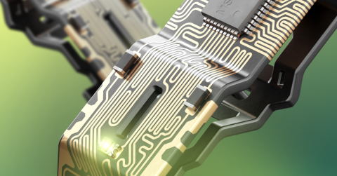
Hello everyone, my name is Tuomas Heikkilä. I am a Senior Hardware Specialist at TactoTek, where we specialize in IMSE electronics. IMSE stands for Injection Molded Structural Electronics. In a nutshell, this technology combines printed electronics and injection molding to create entirely new kinds of products.
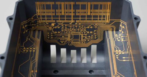
Here’s an example: on the A-side, we have decorative printing, while on the B-side, we integrate the electronics—everything is encapsulated within the plastic. I will explain this in more detail during my presentation today, titled Is ECAD IMSE Ready?
The core focus of this presentation is that since we are working with a new kind of electronics, the requirements for design tools are different.
First, I will go through a few slides introducing IMSE technology and highlight the key differences between IMSE electronics design and traditional PCB design. Then, I will walk you through some real dielectric challenges we have faced in production due to the limitations of standard PCB design tools for IMSE electronics.
Next, we will explore the specific requirements for IMSE design tools, and finally, I will demonstrate how we use Altium and its Printed Electronics Extension to design IMSE electronics.
Understanding IMSE Technology
As I mentioned, IMSE combines printed electronics with injection molding. The process begins with printing: we start with a clear plastic film, print decorative inks, print wiring, and can also integrate features like touch electrodes and antennas. This printing is done using standard screen printing methods.
After printing, we proceed with surface mounting. We place SMD components onto the printed electronic circuit while the film is still flat. This allows us to use standard pick-and-place machines for component assembly. Additionally, we use a standard reflow process; however, since the materials are different from traditional PCBs, the manufacturing parameters must also be adjusted accordingly.
After SMD assembly, we move on to the forming stage. We place the printed film with components into a thermoforming machine, where it is heated until it relaxes. Using vacuum pressure, the film is pressed against a forming tool, taking its final shape. The result is a fully formed film with the printed electronics and components securely in place.
Following the forming process, we proceed to injection molding. In a typical injection molding setup, we use a decorative film with colored inks to create the visual appearance of the part, along with an electronic film that contains the circuitry and components. These films are placed into an injection molding tool, and the molding process encapsulates them.
Here, I have two samples: the first one is without the decorative film, and the second one includes the decorative film. Both are functional parts, and after this presentation, we can power them on to see how they perform in practice.
But this is IMSC in brief. Now, let's go into more detail about the electronics design of these parts and what it actually means in terms of electronics design tools.
Challenges in IMSE Electronics Design
Before we started using Altium and its Printed Electronics Extension, we designed IMSC electronics with standard PCB design tools. However, these tools are optimized for PCBs, as we know. The main point is that in PCBs, we have a dielectric substrate with laminated copper planes on both sides, and the structure always remains similar. Regardless of the number of layers, there is always a dielectric substrate isolating the conductive planes, and PCB manufacturers know how to fabricate PCBs without requiring specific dielectric design files. Of course, we need to specify dielectric materials, thicknesses, and other parameters, but we don't need to share dielectric layer design files for manufacturing.
However, this is not the case with IMSC. In IMSC, the substrate serves as the base on which we print conductive inks and dielectric inks on top of the film. In IMSC, we use local dielectrics, meaning they are printed only in crossover areas.
Because of this, we must design dielectrics in the same way we design conductive traces and conductive layers. This means that for IMSC manufacturing, we must provide both conductive layer files as well as a dielectric design file or manufacturing file. This is the fundamental difference between IMSC and PCB design tool requirements.
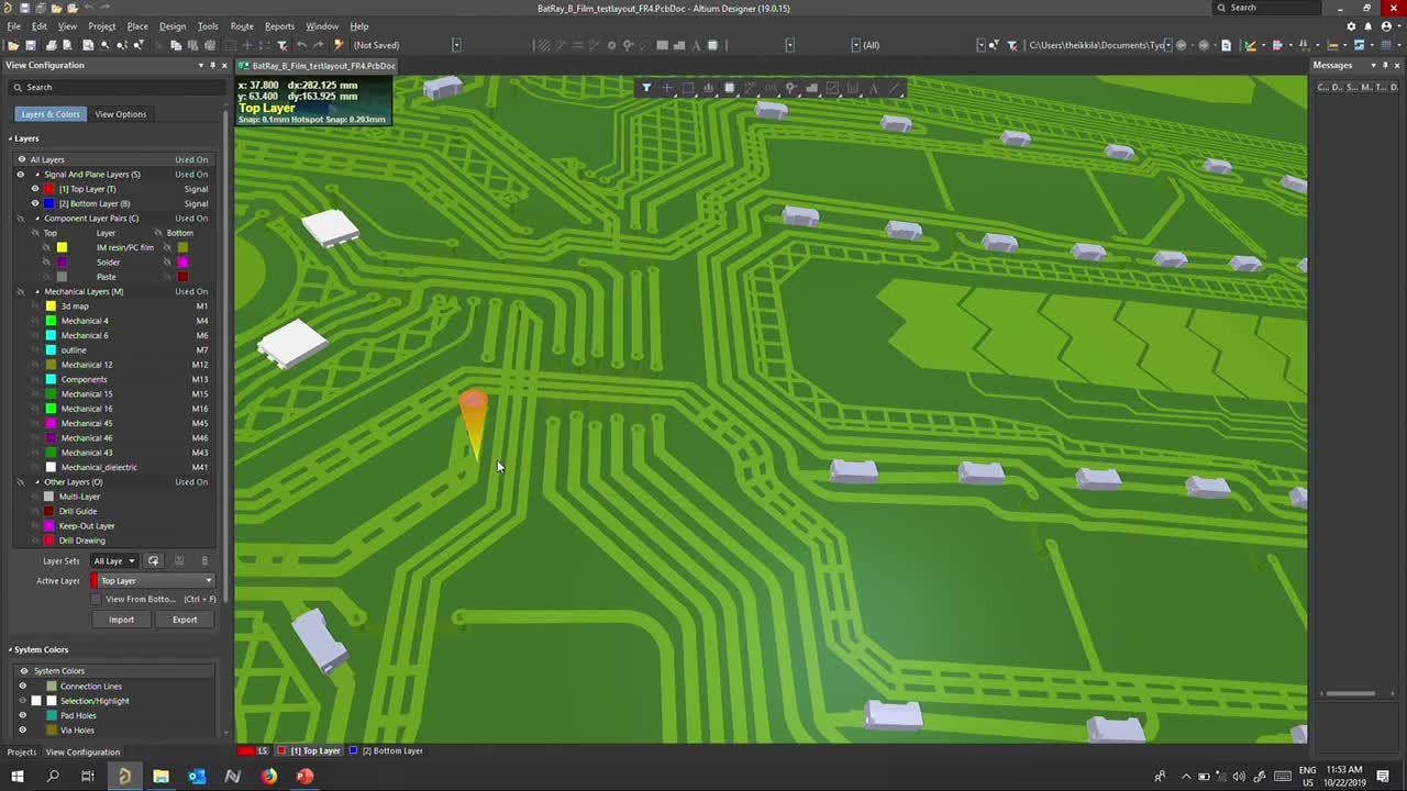
When we attempted to create an IMSC layout using PCB design tools, we encountered numerous failures related to the dielectric. Here, you can see one of our layout designs or a screenshot of it. This is a two-layer design, where two conductive layers are separated by a yellow dielectric layer.
I have highlighted the most common failures we encountered in our production due to the lack of a tool that could properly report dielectric design issues. Let's take a look at the types of failures we experienced.
The first one is here—this is a short circuit at this point. This type of failure was caused by the PCB design tool. We created a slightly wider ground area, and when I used a polygon to define the ground, the PCB design tool automatically generated a polygon area that followed this shape, causing a short circuit. In PCB design, this would not be considered a failure, but in IMSC and printed electronics, it results in a short circuit at this point.
The second type of failure is a missing dielectric, which is caused by human error. When we have hundreds of dielectric elements in our design, manually checking each one visually is quite tedious and error-prone. This method carries a high risk of human errors. Even though the design rule for dielectrics is very simple—placing dielectric material only at crossover points—this type of failure is still very common.
The third type of failure looks like this: we have a dielectric covering nearly the entire crossover area, but it is still insufficient, resulting in a short circuit around this region.
Typically, these kinds of failures occur because, initially, the engineer correctly designs the dielectric to fully cover the crossover area. However, later on, due to an accidental mouse click or some other unintended action, the dielectric shifts away from the crossover area. Detecting these types of failures in the layout is quite difficult through a visual check alone.
The last type of failure occurs when the dielectric fully covers the crossover area, but the expansion is too small. This means that even a slight misalignment between different printing layers could cause a short circuit in this area. Of course, we have methods for aligning different printing layers, but there is always some tolerance—it is never zero. We must allow for small shifts between printing layers by designing dielectrics properly.
These are the types of failures we observed in our production when designing IMSC electronics using PCB design tools. We quickly realized that we needed IMSC-specific design tools to support our design and manufacturing process. While this is not the full specification of what we need, I have highlighted the most important requirements here.
IMSE-Specific Design Requirements
The first and most important requirement is dielectric design. The tool must support dielectric design by providing dedicated layers for dielectrics. We should be able to export manufacturing files for production and define dimensions, dielectric design rules, and other relevant parameters.
The second requirement is IMSC layout design rule checking. While we can utilize many PCB design rules in IMSC electronics design—such as clearance rules, dimensioning, wiring, and keep-out areas—we also need IMSC-specific design rules. Dielectric placement is one of these rules. The rule-checking function should verify all points where dielectrics are required.
Additionally, we have IMSC-specific clearance rules. For example, if we print two parallel traces on different layers and apply the exact same design rules as if they were printed on the same layer, issues may arise. In alignment, these traces are effectively parallel to each other, even if they are on different layers.
The third requirement is a material database, which is also quite important because IMSC layouts are designed for specific inks. During layout design, we specify conductive inks and dielectric inks. If we change the inks, we may need to modify the layout accordingly.
Additionally, when performing electrical simulations—such as checking resistances—we must account for the fact that conductive inks have a much higher resistance than pure copper. Because of this, we need to simulate resistance, and if the materials used in simulation differ from the materials used in production, the final product will not match the original design.
The fourth requirement is a layer stack manager, which is closely related to the material database. We should be able to select the correct materials from the database for our layer stack. In addition to this, we should be able to define the printing order, specify conductive and dielectric layers, and set critical parameters such as trace thickness and other key specifications.
This represents the minimum set of requirements for IMSC electronics design. Altium, along with its Printed Electronics Extension, meets these requirements very well. In fact, we were able to transition our IMSC electronics design from a PCB-based approach to one that is much closer to real IMSC electronics design.
Next, I will discuss Altium, focusing on dielectric generator design rule checks, the IMSC layer stack manager, and the material database.
IMSE Design in Altium
Here, you can see one of our layout designs. In fact, this is exactly the same design as the one shown earlier, where the inner part was circulating around the room.
Initially, this design was created like a PCB. If we switch to 3D view, we can see that it follows a PCB structure—there are traces on the top side of the PCB and also on the bottom side, with vias connecting the traces between layers.
Now, if we return to layer design mode and run a design rule check, I have predefined the design rules based on specifications from our trusted PCB vendor. Running the design rule check against these rules shows no failures in our design. However, we know that this design is actually for IMSC electronics, and there are failures that the PCB design tool does not detect.
For instance, we do not have dielectrics designed for crossover areas. We can try adding dielectrics manually by placing them on a mechanical layer, like this. However, we know this does not actually help our design. If I run the design rule check again, it does not matter whether we have the mechanical layer drawn or not—the tool still does not recognize the dielectric requirement.
To properly transition this design into printed electronics mode, we need to modify the layer stack. We can do this using Altium’s Layer Stack Manager.
In the Layer Stack Manager, we can see that the current setup follows a PCB stack-up structure. To modify it for IMSC, I change the material settings to printed electronics mode and disable rigid-flex. Now, we have a slightly different stack-up:
- Two conductive layers
- One non-conductive dielectric layer placed between the conductors
Next, I rename the layers according to our IMSC naming conventions:
- First conductor (bottom layer)
- Dielectric layer (middle layer)
- Second conductor (top layer)
With these layers properly defined, we also need to specify the printing order. However, we are still missing the material definitions.
To assign the correct materials, we use the Material Database in Altium. Here, we have a selection of printed electronics materials, including conductive and non-conductive options.
For conductive materials, I have created two example conductive inks:
- High elongation ink
- High conductivity ink
Additionally, I have defined an example dielectric material.
Now, we apply these materials to our design:
- First conductor: We select high elongation ink, as it needs to stretch during forming.
- Dielectric layer: We select our predefined dielectric material.
- Second conductor: We apply the appropriate conductive ink for this layer.
In this example, we can use high conductivity ink because these traces will not be stretched during forming. Now, we have defined our inks for IMSC products.
We still have solder mask layers here. However, in practice, IMSC does not use solder mask layers at all. In this case, I can utilize these layers to represent the plastic materials needed for IMSC.
- The bottom solder mask will represent our polycarbonate film, with a thickness of 0.25 millimeters.
- The top solder mask will represent the injection mold resin, which I set to 4 millimeters thick.
These plastic materials are not actually part of the design rules—Altium does not consider them in the DRC (Design Rule Check). We are only using them for visualization purposes to better represent the final product.
Now, I save my design, and if we switch to 3D view mode, we can see that this is no longer a PCB.
I adjust the colors slightly so we can better visualize the changes. The injection-molded version should be transparent, so I modify it accordingly to ensure visibility.
Now, we can see that this design closely resembles IMSC electronics or printed electronics.
The first noticeable change is that there are no traces on the backside of the film anymore. This is consistent with IMSC, where all traces are printed on the top side of the film.
Additionally, we do not have vias in this design. Instead, we only have overlapping areas at specific points. This means that we print conductive ink on both layers, and because they overlap, they form an electrical connection.
At this point, we still do not have dielectrics, so we need to add them. We can do this using Altium’s dielectric pattern generator tool.
To add dielectrics, I select: Tools → Printed Electronics → Generate Dielectric Patterns
Here, I can define the requirements for dielectrics.
- First, I select whether I want to generate or remove dielectrics. In this case, we want to generate them.
- Then, we specify the dielectric layer. Right now, we only have one dielectric layer defined, so we select that one.
- Next, we define that the dielectric should be placed between the first and second conductor layers.
- Finally, we configure the shape expansion for the dielectric. We can select Auto Mode, which means the tool will use the clearance rule to generate the expansion automatically.
Another option is manual definition. Right now, we are using manual definition, and we need to set a 0.7-millimeter expansion for our dielectric. This means that the dielectric extends 0.7 millimeters in each direction beyond the crossover area.
Next, we can define whether we want one large dielectric or multiple smaller ones. If we set the clearance value to 1 millimeter, it means that if the gap between separate dielectric areas is less than 1 millimeter, the tool will merge them into one larger dielectric instead of creating multiple smaller ones.
With this setup, we can automatically generate dielectrics in our design.
Now that the dielectrics are placed, I realize that I forgot to show one thing. So, I will remove the generated dielectrics to demonstrate it properly.
Since we have now changed our design to printed electronics mode, Altium applies printed electronics design rules to this layout. If we run a design rule check (DRC) now, it takes a moment to process.
Even though we haven't made any actual modifications—other than switching from PCB mode to printed electronics mode—we now see a lot of failures in our design.
Upon closer inspection, we find that most of these failures are related to missing dielectrics. We can also see that even if we draw a dielectric layer manually using a mechanical layer, it does not have any effect on the DRC.
So, if we now generate the dielectrics—which we already did—I will proceed with the same settings as before.
We can see that the dielectrics are placed correctly, and the expansion follows the defined design rules. If we run the design rule check again, we can see that the number of failures has significantly decreased. However, we still have some clearance-related failures. Let’s check what kind of failures we have.
We still see some issues with connections. In IMSC, we should not use a design like this, where routing passes beneath the components. There are two main reasons for this:
- The blue trace and the red pad are, in practice, on the same layer, printed on the film. This means that there is insufficient clearance between the traces and between the trace and the pad.
- During injection molding, there is extremely high pressure applied to the component, which creates a high risk of the blue trace cracking under stress.
To fix this, we need to modify the layout so that the routing avoids this area. For example, we can reroute it to another location, like this.
Now, I modify the layout slightly to correct this issue.
This is our polygon area, so I need to re-pour the polygons. Additionally, we need to add a dielectric layer at this point. We can also create dielectric designs manually. I select the dielectric layer and draw the dielectric area manually. Hopefully, this satisfies the design rules—let’s check.
I save my design, and now we should have dielectrics in the correct positions. I run the design rule check again, and we can see that there are no failures anymore. Now, the layout is ready for IMSC production and also for printing production.
If we check the 3D view, we can see that dielectrics are correctly placed between the first and second printed layers.
Conclusion
The Printed Electronics Extension is a very useful tool for IMSC electronics design. Of course, it is also beneficial for printed electronics design in general. This tool is still extremely useful for IMSC electronics design.
Most importantly, it allows us to:
- Check dielectric placement
- Verify clearance design rules specific to IMSC
- Ensure compliance with IMSC-specific clearance constraints
By using an efficient design tool, we can eliminate unnecessary failures during the design phase, rather than discovering them during production. That concludes my presentation for today. Thank you for joining!
Learn More
Explore how Altium supports printed electronics and enables the integration of electrical circuits with three-dimensional mechanical parts.
Related Resources
Table of Contents
Design to Release, Without the Friction
- Keep reviews tied to the right version
- Reduce handoff confusion and rework
- Spot sourcing and release risk earlier
- Work solo, share when needed
Get Started
Thank you, you are now subscribed to updates.