


Designing Printed Electronics with Altium

At a Glance
Design printed electronics with Altium using purpose-built tools for stack-ups, dielectrics, routing, and manufacturing-ready outputs.


As far as I know, Altium is the first electronics design tool that effectively supports printed electronics design. With this tool, you can create printed electronics designs at the same level as standard PCB designs, with capabilities parallel to them. To achieve this, Altium has developed electronics design features specifically for printed electronics.
With Altium, you can define design rules according to the production capabilities that will be used to manufacture a printed electronics part. You can also design schematics and layouts while ensuring signals are routed correctly, and you can export all the required files for manufacturing.
Before using Altium, I created printed electronics designs with PCB design tools that relied on PCB design rules. Naturally, this created significant uncertainty during the design phase because when a tool didn’t support the required technology, I had to complete all design tasks manually. And when things are done manually, the risk of human error increases. An engineer is often blind to their own mistakes, and releasing files in a hurry further raises the probability of design errors.
Minimizing these challenges requires an effective design tool. The need for professional printed electronics design tools becomes even more critical as design complexity increases and electronics designs are developed for real products.
PE vs PCB Design: Different Design Fundamentals
Even though many PCB design tools are available on the market, none have fully supported printed electronics design. Printed electronics have design fundamentals that differ from traditional PCB design.
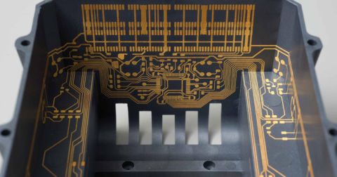
Printed electronics can be made with a PCB-style stack-up, where conductors are printed on both sides of a plastic film and connections between traces are made using vias that penetrate the film.
In this article, I focus on printed electronics in which isolation between conductor layers is achieved by printing dielectric layers.
There are some fundamental differences between PCB design and printed electronics design. In PCBs, there is always a dielectric layer between copper planes, and it appears “automatically” due to PCB construction techniques without requiring a specific design. Traces that change layers are connected by drilling holes through the dielectric layer and plating the drilled hole with copper.
In printed electronics, this is not the case. All layers, including conductors and dielectrics, are printed on top of each other, and the dielectric layer requires a specific dielectric design and corresponding manufacturing files. Without a dielectric layer design, there will be no dielectric material at conductive trace crossovers in the final product.
Printed electronics dielectrics are typically localized, meaning they are printed only at crossover locations. In complex circuits, you may have hundreds of dielectric points, making manual checking difficult. Even a dielectric that is just 0.1 mm too small can cause a short, and identifying this visually in the layout requires zooming in precisely on that point.
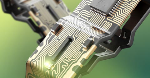
In printed electronics designs, electrical connections between different layers are made by printing a second conductive layer on top of the first conductive layer. There are no real vias; instead, layer changes occur at vias, and printed traces only overlap at these points. For this purpose, PCB design tool vias can be used. A zero-dimensional annular ring via represents the overlapping area of a layer change point in printed electronics.
Design rules for routing differ between PCB design and printed electronics design. Traces printed on different conductive layers follow the same clearance rules as traces printed on the same conductive layer. You cannot place traces too close to each other on the same layer, but similarly, you cannot place traces from different layers too close to each other because different printing layers are only insulated at crossovers.
In printed electronics, traces printed on different layers may be physically adjacent, just like traces on the same layer. The dielectric layer does not provide isolation unless there are crossovers.
Printed Electronics Mode
Altium has a printed electronics mode, and by enabling it, you can design printed electronics with the correct stack-up and DRC (Design Rule Check). In the Layer Stack Manager, you can switch the PCB stack-up to a printed electronics stack-up and define all printed conductive and dielectric layers in the same order in which they will be printed.
In addition to conductor layers, there are dedicated dielectric layers, which are visible and usable in layout design mode as well. In the Layer Stack Manager, you can define ink materials, thicknesses, and critical user parameters for printed layers. Additionally, you can create a database of conductive and dielectric inks, define material parameters, and use these materials in your design.
This mode also enables DRC for printed electronics. When you define the stack-up in printed electronics mode, you also enable printed electronics design rules. Applicable design rules from PCB design tools, such as width and clearance rules, are included, and additional printed electronics design rules are implemented. For example, the previously explained routing design rule is available in the extension.
Dielectric design is supported by the dielectric pattern generator tool. Designers do not need to manually draw each dielectric pattern; instead, the tool checks crossover points and generates a user-specified pattern for each required point. The user can define rules for dielectric dimensioning.
In 3D visualization mode, you can review your layout design as it would appear in a real product.
Printed Electronics Design Flow in Altium
There are many opinions and practices regarding how to create printed electronics. Here, I present my own methods, which I have used in many projects. You can use them as a reference when designing your own printed electronics. Feel free to adopt useful suggestions and disregard tasks you believe are unnecessary.
I begin by creating a project just as I would for PCB design. I create a schematic file, a layout file, and add the required component libraries. I design the schematics according to specification requirements, compile them, and then update the schematics in the layout file. This procedure does not include anything specific to printed electronics. While schematics may require printed electronics-specific solutions, the overall design flow remains the same as in PCB design. However, there are significant differences when designing the layout.
First, I typically define design rules in the PCB Rules and Constraints Editor. These rules must be applicable to the production equipment used for manufacturing the design.
Next, in the Layer Stack Manager, I change the design type from PCB to printed electronics. I define the conductive and dielectric layers, name them, and arrange them in the correct printing order. If I am aware of critical parameters that are important for production and must be documented, I define them for the ink layers. For example, the target thickness of the printed ink, the manufacturer, and the manufacturer’s part number for the inks used are important details to include.
Descriptive names for ink layers help with layout design because the same names are applied to the layer names in the layout design view (PcbDoc). If the name includes the printing order, it is easy to check directly from the name. If an ink has a special characteristic, such as high conductivity, I include that in the name as well.
Next, I define the product outline (layout area), typically by importing the outline drawing from mechanical CAD into Altium. After this, I place critical components (such as LEDs) in their correct positions within the layout area. If the design requires printed sensors or antennas, these are drawn at the beginning as well. I then determine the optimal location for a connector to external systems and reserve an area for contact pads based on the chosen connection method.
For routing, I need to identify all restricted areas, such as mechanical holes to be made in the substrate film, and I mark these on a mechanical layer. Additionally, I must identify and mark all mechanical, optical, graphical, and other features that impose limitations on the electronics layout.
Once these preparations are complete, I begin drawing the layout. The defined design rules and DRC ensure that I do not create a design that conflicts with manufacturing constraints. Furthermore, I need to verify that the routing meets electrical requirements— in printed electronics, this includes accounting for trace resistance.
When routing is complete, I review my original ink selections to assess whether the designed layout, using the selected inks, meets electrical requirements. If not, I must return to either the Layer Stack Manager or the layout to analyze which aspect needs modification— whether the inks, the layout, or both.
The final step is to create dielectric layers to insulate crossover locations. In Altium, I use the dielectric pattern generation tool, which performs this operation quickly and accurately. I simply define the expansion area for the dielectrics (how far they extend beyond the conductors) and specify the conductive layers between which dielectric insulation is required.
Once the layout is complete, I run a DRC check.
Preparation for Manufacturing
Preparation for manufacturing in printed electronics requires special attention because the performance range of materials can vary significantly, and material processing methods affect the electrical characteristics of conductive inks. Design files and documentation should be detailed to ensure that there is only one possible way to manufacture the design.
All materials, their manufacturing methods, and parameters must be clearly defined. Similarly, the stack-up, including the correct inks and printing order, must be explicitly specified, and the layout must be designed using the correct design rules.
Strive to create documentation that eliminates any possibility of misunderstanding how the printing process should be executed.
When the printed electronics layout is complete, it makes sense to panelize the layouts within the printing area. In the panel file, I add the necessary fiducials and reference points for the pick-and-place (component mounting) process. I then export the fabrication files in the format required by the CAM engineer.
I export the stack-up file from Altium or carefully prepare a separate stack-up document. Assembly files are generated in the same way as for PCBs. At a minimum, the pick-and-place file and the parts list are required.
In practice, preparation for manufacturing involves sharing files and documentation across multiple platforms. Keeping everything organized is much easier when you rely on Altium, as it provides centralized file management, real-time collaboration, and seamless integration with manufacturing processes. Schematic and layout files serve as the working documents containing all electronics-related items, including materials, components, stack-up, printing order, and more. This ensures that all design choices are accurately transferred to manufacturing.
Following the process I’ve described requires a professional printed electronics design tool like Altium.

About Author
Related Resources
Table of Contents
Design to Release, Without the Friction
- Keep reviews tied to the right version
- Reduce handoff confusion and rework
- Spot sourcing and release risk earlier
- Work solo, share when needed
Get Started
Thank you, you are now subscribed to updates.

