Intelligent Routing Features In PCB Design Software Let You Work Smarter, Not Harder
Everybody has those lazy moments, trying to figure out how little one can do while still completing a task. In my first job, I created software where I can automatically launch my favorite applications through voice commands. Later, I found a new level by coding a special program to email reports, close applications, and shut down my computer with one click of a button.
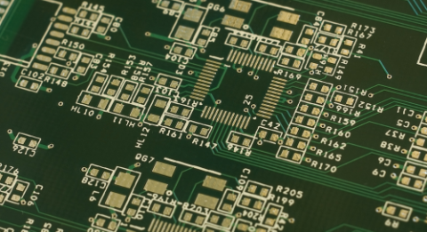
My first PCB designs took place on the early versions of PCB design software. These had auto-routing capability; however, I didn’t know how to use them very well yet. I thought, like with my end-of-the-day app, I could just hit a button, go grab some tea, and have the PCB ready for manufacturing when I came back. Yeah, imagine the disappointment when I come back to a poorly routed PCB that I then have to spend hours reworking. It wasn’t very fun.
A decade later, PCB design software has gone through many cycles of revision and improvements. Today’s intelligent routing features in PCB design software are much more powerful than their predecessors. But another part of their improving usability is my growing knowledge and experience: PCB software was never meant to replace the skill and insights of a hardware engineer, and so it wasn’t built to do that. Instead, PCB design software, when used appropriately, can save hardware engineers precious time to complete their design. Four key tools can help you leverage intelligent routing features in PCB design software without falling into complacency.
1. Component Auto-Placer
The component auto-placer is a great tool that arranges all your components systematically. It is tempting to just use the auto-placer on most of your components and start the routing process. Indeed, in a simple design, there may not be any major issues. However, in complex applications, failing to separate components according to their modules may cause cross-coupling between noisy components and analog circuits. When cross-coupling occurs, the components end up polluting each other and the system in place, changing an isolated interaction to a more problematic disturbance.
The component placement must take into account several factors, including heat production and sensitivity as well as the direction and orientation of signals. While it may be possible to have an auto-placer work with these considerations in mind, it is more important to maintain a compatible relationship with the auto-placer. The auto-placer is best used to complement the best practice of component placement.
2. Auto Router
Following my—failed—attempt to have the intelligent autorouting feature take over my job, I’ve changed my way of using this intelligent routing tool. Now I use the auto-routing tool to save me countless hours of routing an “unroutable” board.
Unroutable boards often occur when your board is too small to hold the number of required connections. When you’re working in this situation, a quick test to save you time is to hit the auto-route and see if it can complete the routing in its first two attempts. If the auto-router fails, then you might need to revise your components or enlarge the PCB size. If you were to attempt this test manually, you could be wasting valuable time. Worse yet is designing before running the auto-route: in that case, you might spend hours on a PCB design just to find that it is impossible to route given its size.
One of the best tactics for using eCADSTAR intelligent autorouting is to apply it alongside manual and interactive routing. Begin by placing the power supply, high-speed communication, and analog signals manually. Then route the differential pairs before completing the remaining signals with the auto-routing tool. Make sure that the auto-route signal does not alter pre-routed important tracks.
3. Multiple Pair and Differential Pair Routing
The multiple pair and differential pair routing are great tools for maintaining equal copper length and ensuring they are running in parallel. Instead of routing one signal followed by others, it saves you precious time by routing a set of signals simultaneously. As intelligent as it is, however, it is up to you as the designer to ensure that the differential or multiple pairs signal is not routed near other high-speed or analog signals. Consider multiple pair and differential pair routing as tools in your toolbox rather than a replacement for your engineering insights.
4. Design Rule Check
Design rule check (DRC) is probably the best tool that helps engineers to eliminate human errors. It highlights routing errors and zooms into the exact location on the PCB for immediate remedial work. As great as it is, it shouldn’t be the cause of complacency in engineers where PCB best practices are concerned. While it may help eliminate mistakes like unconnected nets or clearance constraint violations, compatibility with both features and experience will allow the engineer to identify issues like ground loops or incorrect ground plane placement. Ultimately, the DRC is only as effective as the engineer who configures it.
When you need to access an easy-to-use PCB layout tool that includes everything needed to build high-quality manufacturable circuit boards, look no further than CircuitMaker. In addition to easy-to-use PCB design software, all CircuitMaker users have access to a personal workspace on the Altium 365 platform. You can upload and store your design data in the cloud, and you can easily view your projects via your web browser in a secure platform.
Start using CircuitMaker today and stay tuned for the new CircuitMaker Pro from Altium.


