Keep Your PCB Assembly and Production Processes Like Your Best Pants: Seamless
I lost a button on an old pair of jeans the other day and I was totally unable to repair it. The seams were all sorts of wonky, and while normally you can find extra buttons along the waist there were none to be found. My mom taught me to always check the seams, but sometimes it’s easy to get lazy and forget to do some of the most basic procedures when you want to get an otherwise grueling experience done with. Some brands are more trustworthy and reliably durable than others, but even then it’s still a good practice to check the clothes you’re about to buy for any obvious manufacturing defects.
In an ideal world, all the most rigorous checks are outsourced back to the manufacturer. After all, they’re directly involved in the production process and should have the equipment to review themselves with ease. In a realistic world, your PCB manufacturer should be doing all the necessary inspection and process checks. Being able to verify these processes are happening is a critical component of your manufacturer relationship. With the right knowledge, you’ll know what to look for and ask about when verifying manufacturing procedures as well as ensuring some initial product testing.
Why Inspect Your PCB Assembly and Production Processes?
Inspecting a manufacturing facility will enable you to develop a more trusting rapport with your manufacturer as well as give you confidence that your manufacturing choice is the best for your design considerations. When you visit your manufacturing facility, you should check all of the tools and facilities that will be used to produce your board. You also want to look at handling between tools, and materials being used. However, your work is far from done once you’ve verified all the tools for a build.
After assembly, and probably at several stages of fabrication, your manufacturer should be inspecting the boards and conducting process checks. Ideally, they will even be able to do some function tests and find any issues before the final boards are shipped back to you. After all, if your pants were being sewn with a hole instead of pockets you would want that to be found early so the pockets could be replaced easily.
What Are Your Methods of Inspection?
Using the fabrication flow path for your PCB and the processes that are activated during manufacturing, you can determine inspection tools and procedures. You should find out about the following inspection processes used by your manufacturer, and watch them in action if you can:
Mechanical inspection: Some mechanical tests include shock and thermal creep, but regardless of what (if any) additional stress you apply to the boards, it should still be physically intact and undamaged before you send it out.
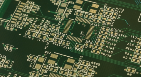
Optical inspection: Looking at the boards with a bare eye or under a microscope allows you to inspect for larger scale physical damage. Solder bridges, burns, and misalignments from reflow are usually easily visible if you have the patience to search.
Adhesion testing: If the mix of materials in the layer stack doesn't have the right ratios, you can have delamination between the copper and the laminate or the solder mask. This should be checked during manufacturing; if you discover it later you may have to scrap many and many more hours of fabrication work. An adhesion test is often as simple as putting scotch tape over a layer and checking that nothing from the board gets peeled up with it.
SEM inspection: Scanning electron microscopes (SEM) are another very expensive piece of equipment. If you have extraordinarily fine features, the SEM imaging might be used to inspect the board. However, it’s more often used to evaluate metallization. The electron beam will damage certain types of materials, even stripping them away. Gold-coated pads are tested this way, with a fast stripping time indicating a very thin plating layer and revealing a poor surface quality.
X-Ray inspection: If there are issues with opens or shorts after the layer stack up has been fabricated, a non-destructive testing option is preferable until you know for sure what and where the problem is. Not every manufacturing plant has x-ray inspection capabilities, so it's something you should ask about when you visit.
How Much Can Your Manufacturer Test?
The testing that can be done by your manufacturer varies, but at a minimum, they should have some rudimentary electrical testing and thermal imaging to find areas of high-current draw (indicating leakage). Ideally, they’ll also have electron microscopy or the capability to do elemental analysis, which can be used to drill down deeper into identifying the root cause of an electrical issue.
If you have specific standards you need to meet, like MIL-SPECs, or consumer safety requirements, you should also find out if there’s any pre-compliance testing that the manufacturer can attend to. If they can produce and test an initial batch it will be much cheaper than finding out in the middle of certification that you’ve got a mysterious resonance or can’t meet voltage safety requirements.
While it’s admirably gutsy, and maybe saves you a little time in the present, buying jeans without trying them on is just asking for trouble in the future. Having PCBs produced without being familiar with your manufacturer isn’t even admirably gutsy, it is going up to trouble’s doorstep and begging for it to come visit you.
By choosing the right PCB design software, you can select the tools that will save you in the long run and ensure quality, repeatable processes. When you need to access an easy-to-use PCB layout tool that includes everything needed to build high-quality manufacturable circuit boards, look no further than CircuitMaker. In addition to easy-to-use PCB design software, all CircuitMaker users have access to a personal workspace on the Altium 365 platform. You can upload and store your design data in the cloud, and you can easily view your projects via your web browser in a secure platform.
Start using CircuitMaker today and stay tuned for the new CircuitMaker Pro from Altium.


