

Moving to Altium Designer from KiCad


KiCad users have access to an open-source platform that users can adapt and customize to their own workflows as long as they have some software experience. However, KiCad has been continuously developed without critical integrations into enterprise systems or automation systems focusing on volume manufacturing and lifecycle management. This is why it tends to occupy the hobby and maker spaces and only now is including features available in paid PCB design software a decade ago.
These features that go above and beyond KiCad include:
- Automated placement features that expedite PCB design
- Automated routing features that are required for advanced digital designs
- Managed libraries with direct links to supply chain inside the library data
- Instant access to component lifecycle statuses in libraries and in the BOM
- Automated documentation generation for volume manufacturing deliverables
- Integrations into MCAD software for instant error-free collaboration with mechanical designers
- Integrations that support volume builds and ongoing revision control (e.g., PLM systems, ERP, MRP, etc.)
As soon as you intend to move up the value chain in the electronics industry, free platforms like KiCad are totally unable to keep up. They can't handle the basic documentation, collaboration, and management tasks that are demanded in real products.
That’s the core reason many designers treat a paid EDA software seat as an investment rather than a cost. The value isn’t just “more features,” it’s the ability to access projects and clients at the enterprise level.
Cost is also often misunderstood. When you compare the pricing of enterprise PCB design platforms, Altium is frequently positioned as a practical step up: it offers all the workflow features you’d expect in higher-tier tool suites without forcing you into the kind of licensing costs you find in platforms like Siemens and Cadence. For an individual designer, consultant, or growing team, that matters: it makes the highest-value professional design experience attainable earlier in your career.
What Projects Can You Pursue In Altium Designer?
Whether you're an innovator building a startup, independent freelance designer, or you run a design services firm, you can pursue any project you like, including enterprise-level projects that carry the highest value.
Most importantly, using the same toolchain that many professional teams standardize on tends to expand the set of projects you can credibly pursue. Clients and employers who care about manufacturability, documentation quality, collaboration, and lifecycle management, which includes many of the world's largest and highest-paying companies, expect you to work in an environment that supports those requirements out of the box. If your goal is to move up the value chain, getting away from Arduino clone boards and into production hardware and long-lived products, your PCB design software is a major part of that transition.
Companies in every industry use Altium Designer, including today's high-value industries developing advanced products:
- Defense and aerospace
- Advanced industrial equipment
- Robotitcs and autonomous systems
- Automotive
- Energy and grid infrastructure
- Medical devices
- Data center infrastructure
If you want to make the shift to Altium Designer while leveraging your current set of design data and library components, Altium makes the migration process easy.
Making a Smooth Transition to Altium Designer Develop from KiCad Layout
In this guide, we’ll focus on importing KiCad Layout PCB designs. Please refer to specific guides if you need to migrate other files.
Legacy Translation
Before You Begin
This guide will show you how to import data from your legacy system into Altium Designer Develop. Before importing all of your legacy data, it’s important to ask yourself, “why do I need to import my legacy data?” Below are some of the most common considerations to consider when deciding whether to import legacy data into Altium Designer Develop.
"We have 20 years of data, and I don’t want to leave it behind.
- Does the legacy data include critical information for creating robust designs within Altium?
- Is it easier to start new designs rather than re-work the imported data to make it usable?
"Our service bureau doesn’t use Altium, but they can import Altium data. Our Altium system can import their data. Is this a reliable way to pass designs between our companies?.
- How do you maintain library integrity?
- Who has design authority?
- How do you plan to verify the data?
"We have some ‘golden’ designs that we need to bring into Altium Designer Develop so that we can up-issue them.
- How do you plan to verify the imported data?
- How much re-work is going to be needed after importing?
- You need to take advantage of additional Altium Designer Develop features once the data is imported?
"We have a library of trusted parts which we’d like to bring into Altium.
- Are there any exotic parts that you may have trouble representing within Altium?
- Do you need to add Altium-specific features (like 3D models) for every part?
- How much redundancy, duplication, and error is present in your library?
After reviewing these considerations, read on to learn how to import your legacy data into Altium Designer Develop.
Preparing to Migrate Your Legacy Data
There are four phases to migrating legacy data.
1. Prepare original data
|
2. Export data
|
3. Import data
|
4. Post import
|
Phase 1: Prepare Original Data
It is prudent to clean up your design before attempting to export. Below is a checklist of data cleanup best practices to help you as you prepare your data:
Schematic considerations:
- Individual pin connectors (example: Block connectors) in KiCad must be modified at the KiCad tool level before migration. Alternatively, you can replace pin connectors in Altium Designer Develop post-migration.
- Connectors should be represented as one-gate-per- pin with over 256 “gates.”
- Ambiguous connectivity for reuse blocks must be broken apart in KiCad.
- Remove hidden pins or implicit connections.
- Local net names placed at wire intersection must be placed at correct locations (away from intersection point)
- Are schematic symbols mapped to correct PCB footprints?
- Schematic and PCB are in sync?
PCB considerations:
- Large numbers of graphical objects like mechanical drawing or non-ECO-registered drawing primitives must be migrated on documentation layers.
- Perform a star point grounding check.
- Remove deliberate DRC violations.
- Remove objects extending beyond the environment.
- Known PCB layer assignments need to map correctly with existing Altium Designer Develop PCB, especially with the power plane or signal layer.
- Do the auto-named nets match with the schematic?
- Remove dimensions in KiCad PCB(Ver. 6.0x)
Library considerations:
- Do the schematic symbols match with PCB footprints?
- Does the library contain correct supply chain information and BoM parameters?
- Does 3D information need to be imported? If yes, then the height attribute should be assigned in KiCad.
- Check for correct representation of custom pads, copper shapes, solder mask, and resist.
Phase 2: Save Data in a Suitable Format
Supported Version and File Format
The following table shows KiCad PCB Design Formats and versions that can migrate into Altium Designer Develop. This list is updated regularly, so please check with us before starting a new migration. Refer to this link for updated information.
TYPE | SYSTEM | VERSION | FORMAT |
Project | Project | 6.0x | ASCII (*.kicad_pro, *.pro) |
Schematic | Schematic Editor | 6.0x | ASCII (*.kicad_sch, *.sch) |
Schematic Symbol | Symbol Editor | 6.0x | ASCII (*.kicad_sym, *.lib) |
PCB | PCB Editor | 6.0x | ASCII (*.kicad_pcb) |
PCB Footprint | Footprint Editor | 6.0x | ASCII (*.kicad_mod, *.lib) |
Layout/PCB and Schematic files translate to Altium Designer Develop as follows:
KICAD FILE TYPE | ALTIUM DESIGNER DEVELOP FILE TYPE |
KiCad PCB (*.kicad_pcb) | Altium Designer Develop PCB files (*.PcbDoc) |
KiCad Schematic (*.kicad_sch, *.sch) | Altium Designer Develop Schematic file (*.SchDoc) |
Schematics and PCB files will grouped be and placed in an automatically-created Altium Designer Develop project (*.PrjPCB).
For more information on linking files together to allow for cross navigation and ECO generation, check out the “Component Links” section in our ‘Bringing Together Imported Schematic and PCB Designs’ guide.
Library files translate as follows:
KICAD FILE TYPE | ALTIUM DESIGNER DEVELOP FILE TYPE |
KiCad Schematic Symbol (*.kicad_sym, *.lib) | Altium Designer Develop Schematic library files |
KiCad PCB Footprint (*.kicad_mod, *.lib) | Altium Designer Develop PCB library files (*.PcbLib) |
Phase 3: Import Data into Altium Designer Develop
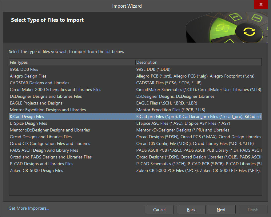
Using the Import Wizard for KiCad Files
You can launch the Altium Designer Develop Import Wizard from the File menu.
- Choose the KiCad Design Files option, as shown below.
- On the “Importing KiCad Designs” screen, click the Add button to choose Layout or Logic files.
- You can translate multiple files at the same time.
- Step-by-step instructions on using the Import Wizard follow next.
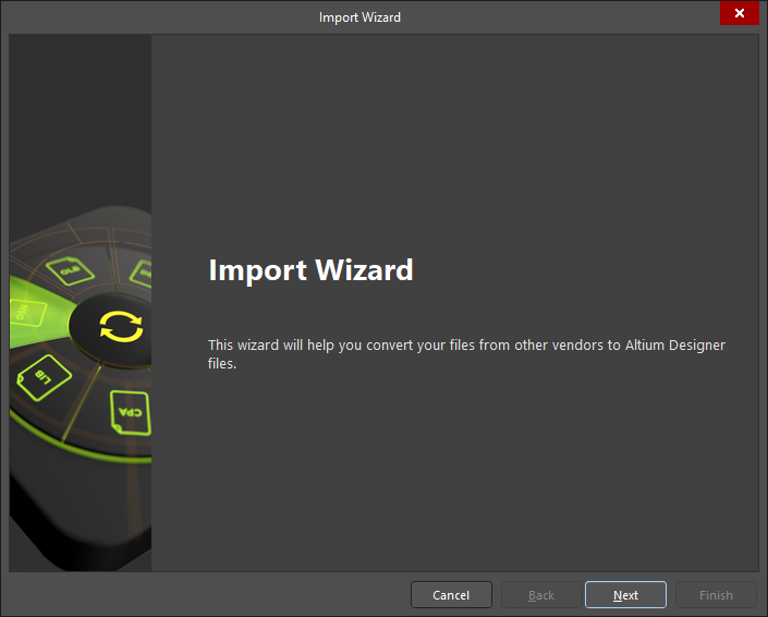
Starting the Import Wizard for KiCad Files
Step-by-Step Import Instructions on Importing a KiCad Design file
- Start the Import Wizard with File » Import Wizard
- Select Type of Files to Import—>KiCad Designs Files.
- Add the file(s) to be translated. In this case, the “CM4IO-KiCAD” file has been used.
NOTE:
You can add as many KiCad Design files as you like at this point. However, if you add files of a different name, then separate projects will be created.
- In the next step you can add your Symbol/Footprint Library Files to import (if available).
- Set the options for what level of reporting is done after the translation has been completed.
- Check the errors and warnings in Messages.
- A preview of the files being translated, and their output directories are shown. You can change the main output directory if desired.
- Set the schematic import options.
- Set the PCB import options.
- Map KiCad board layer to Altium Designer Develop board layer.
- Click the final Next button and the Import Wizard will take care of the rest.
- Congratulations! Your design has been imported into Altium Designer Develop!
- Follow the Post Import Tidy Up checklist to ensure the design has been fully reviewed and verified.
- If you would like detailed information on how to carry out some of the tidy-up checks, please review our ‘Bringing Together Imported Schematic and PCB Designs’ guide.
Phase 4: Post Import Tidy Up
Once your migration is complete, we recommend checking your design to ensure that all data is transferred as expected. Below is a list of key checks to perform post-migration:
Physical check
- View » Fit Document
- Board shape and cutouts
Electrical check
- Netlist
Rules
- Have all rules been imported
- DRC check
- Check settings for polygons - Island removal, min primitive size
- Thermal reliefs, direct connect
- Check power plane settings
- Power plane Pull-back
- Solder mask, Paste mask rules
- Via Tenting
- Testpoint assignments
Power check
- Nets
- Planes
- Polygons
Documentation check
- Layers
- Text/Strings
- Legends
PCB reports
- Number of components/nets
- All nets routed
Getting Help
There are many ways to learn more about Altium Designer Develop:
- F1 over any object, editor, panel, menu entry, or button to open a brief description in your web browser
- Press Shift+F1 or ~ key while running a command for a list of shortcuts you can use in that command.
- Access our complete Altium Designer Develop Documentation online.
- Visit the Altium Video Library where you can watch training on over 150 different topics. Each video walks you through the steps needed to complete a task.
- All Altium Designer Develop subscription levels include easy access to real-time support, user communities, comprehensive product documentation, training videos, and knowledge base of targeted solutions for common user experiences. Contact Altium Support Here.
Additional Resources
Online Resources:
If you’re ready to dive deeper into the powerful features of Altium Designer Develop, below is a list of articles that
provide information to help you get started.
- For a full overview of the PCB design process with Altium Designer Develop, check out this tutorial: A Complete Design Walkthrough with Altium Designer Develop.
- For a look at the basics of creating components, read A Look at Creating Library Components.
- For a tutorial that steps you through all the basics of editing multiple objects, take a look at Schematic Placement and Editing Techniques in Altium Designer Develop.
- For an overview of How to Start an FPGA PCB Layout in Altium Develop Designer, read How to Start an FPGA PCB Layout For Your Embedded System.
Software Platform Resources:
Another great way to get the most out of your Altium Designer Develop installation is by exploring its help section. You can launch the help menu on the left side of Altium Designer Develop by clicking Help and navigating to Exploring Altium Designer Develop.

About Author
Table of Contents
Design to Release, Without the Friction
- Keep reviews tied to the right version
- Reduce handoff confusion and rework
- Spot sourcing and release risk earlier
- Work solo, share when needed
Get Started
Thank you, you are now subscribed to updates.

