


Rules Verification in Agile PCB Design and Development
Agile development relies on a unique workflow that can benefit from PCB design rule verification
I used to think that agile development is just a software development methodology with specific rules and processes. Agile hardware design processes seem to be rigid when viewed from the surface, but any agile design process is designed to allow a team to adapt to change throughout the product development cycle. In reality, the central ideas in agile development can be applied to any business process that is at risk of changes, including hardware design.
If implemented correctly, an agile development workflow can help prevent unnecessary redesigns and ensure that a product’s functionality is closely aligned with the customer’s needs. Within electronics and hardware design, the ideas in agile methodologies rely on PCB design rule verification throughout the product development process. This helps a design team quickly validate design requirements and propose design changes during each sprint.
A Rules-Driven Agile Workflow
Agile workflows are designed to be adaptable and adapt to change throughout the design process. The documentation phase at the beginning of any agile development method provides designers with a chance to define important design rules and constraints before design begins. You can encode these rules into your design software at the outset of the design phase. These design rules can follow industry standards for your particular application, or they can go beyond standard rules with the goal of improving the performance and reliability of your product.
Rules and constraints in your design tools help ensure that your schematic design and PCB layout will meet your requirements as you build up your board. Some design software packages only allow you to check your design against your rules and constraints in batches, thus most design processes require design rule checks at specific points during the design process. As part of an agile workflow, it is best to check your design against your rules and constraints during each design sprint as you work toward design milestones.
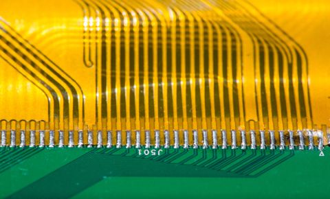
The best design tools will check your layout against design rules in real-time, allowing you to identify errors as you layout your board. Unified interactive and auto-interactive routing tools are perfect in this regard as they check your routing choices against your design rules in real-time. You can immediately identify clearance violations, length mismatch violations, and ensure your traces maintain consistent geometry throughout an interconnect.
Imagine checking every one of these traces against your design rules manually...
These same ideas apply to embedded systems; working with the right embedded software tools can help you quickly identify errors or problems in your code by comparing it with important coding standards (e.g., MISRA and CERT C in TASKING) before you compile your code and deploy it in a prototype.
Overcome the Limits of PCB Design Rule Verification with Simulations
Although design rules are important for ensuring your design will be manufacturable and meet important design standards, design rules do not guarantee the electrical performance of your system. Just because your design meets basic industry standards and manufacturing guidelines doesn’t mean it will provide the electrical performance you require. This is where performing simulations at various points during design can help you identify layout or component changes that can improve signal integrity in your design.
Prior to beginning a new design, simulations of important circuits are normally run in SPICE or another circuit simulator. This is helpful for validating design requirements and proposing changes before beginning schematic design and layout. After validation, a linear design process normally dictates that simulations be performed at specific points (normally once the design is completed). This is in part due to the fact that many simulators exist external to the design software itself, and invoking multiple simulations during the design phase simply takes too much time.
With integrated design software, you can immediately run simulations of your schematic and your PCB layout without exporting your design to an external program. This makes integrated software the ideal choice for agile design as you won’t need to wait until the end of your layout is completed to run simulations. When your simulation tools are integrated into your design software, you can quickly diagnose signal integrity problems during successive design sprints as part of an agile workflow.
Just one of many electrical simulations you can perform in an agile design process
Adapting to Change in PCB Design
Results from simulations inform two aspects of design modification: swapping components and changing your layout. Performing simulations of your device at the schematic and component level help you determine whether the components you have chosen will provide the electrical performance specified in your design requirements. You can then quickly replace components as needed, or you can modify your electronics schematic to solve any signal integrity problems.
Even after a schematic is corrected based on simulation results, you still can’t guarantee performance without PCB design rule verification of your layout. Simulations of your layout are also critical as they can help you identify layout choices that contribute to crosstalk, EMI susceptibility, and other signal integrity problems. As part of an agile workflow, this allows you to identify specific changes that would be required in your layout, allowing you to address them quickly during each design sprint. This is better than waiting until your design is fully completed, as is typically done in a linear design process. In that case, any layout changes can be extensive and time-consuming, and this situation should be avoided whenever possible.
The rules-driven design engine in Altium Designer® can now be integrated with the data management features in Altium Concord Pro™, providing designers with a complete tool set for agile development. The PCB design rule verification features in Altium Designer are built into the standard design features, making them fit perfectly within any agile development workflow.
Contact us or download a free trial of Altium Designer and Altium Concord Pro. You’ll have access to the industry’s best routing, layout, simulation, and MCAD collaboration tools in a single program. Talk to an Altium expert today to learn more.

About Author
Related Resources
Related Technical Documentation
Table of Contents
Altium is transforming the electronics industry so thoroughly that our web pages need a minute to catch up. For a short time, some information on this page may be outdated.
We appreciate your patience. It will be worth the wait!
Learn More
Thank you, you are now subscribed to updates.