
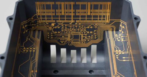


Design Philosophy in Printed Electronics Manufacturing

At a Glance
Optimize performance or manufacturability? Explore key trade-offs in Printed Electronics Manufacturing and how design choices impact resistance, materials, production.


In printed electronics, I approach design philosophy from a new perspective. My key question regarding design philosophy relates to printed electronics manufacturing: Should I optimize my layout for electrical performance or manufacturability, even if that means compromising electrical characteristics?
In printed electronics design, I must make trade-offs between trace resistance, voltage levels, power consumption, and layout area. By properly balancing these factors, I can define the topology of an electronic solution that meets the required functionality. Resistance plays a significant role in this process—not as a feature enabler, but rather as a constraint. The key objective regarding resistance is always to minimize it. Two primary tactics for achieving this are using highly conductive inks and maximizing trace thickness.
While these tactics may seem straightforward, they can introduce challenges related to design for manufacturability. In printed electronics, design for manufacturing is not always obvious, and manufacturing capabilities may not always be well-defined. Therefore, it is essential to assess manufacturing constraints and design the printed electronics layout accordingly.
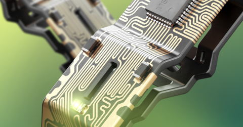
Printing Method Defines Trace Characteristics
Traces in printed electronics can be manufactured using various methods, each with its own parameters for optimizing the electrical characteristics of the trace. One such method is screen printing, which is fast, cost-effective, and easily scalable for high-volume production.
In screen printing, the selected screen is a key factor in defining the dimensions of the printed and cured trace. Typically, reusable screens are prepared for production by adding a photoresist capillary to the screen, exposing the layout image onto the capillary, and then revealing the image by washing away the non-exposed capillary. Together, the selected screen and added capillary determine how much ink is transferred to the film during printing.
Additionally, the thickness of the printed trace directly impacts its resistance. The trace thickness varies depending on the type of screen, capillary, or both. The choice of screen and capillary also sets limitations on the minimum trace width and the minimum clearance between traces. If the production process has a limited selection of screens and capillary options, it restricts the ability to achieve different electrical characteristics.
Regardless of the printing method used, it is essential to understand the parameters that influence electrical characteristics and the potential limitations printing imposes on layout design.
Processing Liquid Materials
In printed electronics, traces are manufactured by processing liquid materials, which solidify during the curing process. The liquid raw material is the most critical factor in determining trace resistance, while the printing process primarily defines the amount of material in the trace. The key "quality factor" in this context is the cross-sectional area of the trace—the larger the area, the more raw material is used, resulting in lower resistance. However, it is important to note that the raw material itself has the greatest impact on resistance.
Typically, compensating for the resistance of a low-conductivity ink by increasing the cross-sectional area is not practical, as it requires significantly more layout space. Instead, from a resistance standpoint, switching to a more conductive ink is more effective than increasing the trace thickness or width. In some cases, ink selection is application-dependent. For example, translucent conductive ink may be used in illuminated capacitive sensor applications where light needs to pass through the electrode. In other cases, highly conductive ink may be required for applications with higher current demands, such as driving LEDs.
In screen printing, ink selection influences how the screen must be prepared and how the liquid ink is processed during manufacturing. This includes setting parameters for the printing machine, such as squeegee selection, printing speed, and printing pressure. The conductive ink chosen for a product impacts both screen selection and the parameters needed to achieve the desired trace dimensions. Ultimately, the combination of trace dimensions and ink properties determines the final resistance values of the trace.
Design for Manufacturing or Manufacturing for Design?
Three critical parameters determine resistance: the selected ink, the thickness of the trace, and the width of the trace. If there is a critical resistance limit and one parameter is fixed, it typically impacts the others. For example, if the conductive ink is fixed and resistance needs to be minimized, the maximum allowable thickness and width of the trace must be adjusted accordingly. Similarly, if layout space is highly constrained and the trace width must be minimized, reducing trace resistance is limited to selecting a higher conductivity ink and/or maximizing trace thickness. Regardless of the choices made in printed electronics design, these factors always influence the printing setup and manufacturing parameters.
Designing for manufacturing (DFM) in printed electronics is more complex than designing a PCB for production. In printed electronics, there are multiple ways to achieve a specific resistance. For instance, the same resistance can be obtained using a thin layer of high-conductivity ink or a thicker layer of lower-conductivity ink. However, these traces will have different current-carrying capacities. Using the same ink, different square resistance values can be achieved simply by varying the thickness of the capillary used in the screen, which affects ink deposition and, consequently, trace thickness. Numerous manufacturing parameters directly impact the square resistance value of a printed trace, and understanding all of them requires extensive experience with printing processes and conductive inks. Poor quality control, inadequate knowledge of ink processing, or a lack of printing experience can result in incorrect square resistance values and significant variations between parts.
An additional complexity, compared to the PCB world, is conductive ink selection. Conductive ink plays a crucial role in printed electronics performance and is a key element of printed electronics DFM. Successfully processing any functional ink during manufacturing requires expertise to achieve the desired results. Ideally, the ink has been validated by the printing manufacturer, who understands how to select appropriate screens, tools, and parameters based on the electrical requirements. If the manufacturer lacks validation data demonstrating their ability to process a specific ink correctly, it introduces significant uncertainty.
All of these factors raise important questions about the trade-offs between electrical characteristics and DFM. What is a reasonable or acceptable level of increased resistance—and consequently, higher power consumption—to simplify the manufacturing setup? Or should manufacturing be pushed to adjust its equipment and methods to meet the electrical requirements?
Requirements for Manufacturing
There are two extreme approaches to designing printed electronics from a manufacturing perspective. The first is to design the layout strictly according to manufacturing limitations and constraints. This approach requires trade-offs between electrical performance and manufacturability based on available production capabilities. The second approach is to design the layout solely for optimal electrical performance and require manufacturing to adjust printing equipment and parameters accordingly. This method avoids compromises in electrical performance, but it demands modifications to tools and processes to achieve the desired outcome. All other design strategies fall somewhere between these two extremes. There is no definitive answer as to which approach is optimal or the "correct" way to proceed. Because of this challenge, my recommendation is to specify critical manufacturing requirements clearly.
Naturally, the application and its specific requirements dictate what is most important in printed electronics manufacturing. Is there a specific ink that must be used? Is trace thickness a priority? Or is resistance the only concern, regardless of ink type or thickness? It is essential to identify the most critical characteristics and define them clearly. Additionally, consider the power budget and determine whether higher resistance can be compensated for by increasing supply voltage levels. Once these key factors are understood, specify the critical characteristics unambiguously and establish controls to ensure they are met during manufacturing.
I have encountered cases where maintaining a specific resistance range with a particular ink was crucial due to high current requirements and a limited power budget. In another case, the driver voltage was high relative to the current, making ink type and resistance less critical as long as the ink was silver-based. In all scenarios, voltage loss in the trace was so minimal—even when using a thin layer of low-conductivity silver ink—that it was negligible. Naturally, the manufacturing requirements varied between these cases. The first required strict production controls, while the second allowed for greater flexibility.
The design philosophy of printed electronics revolves primarily around trade-offs between manufacturing capabilities and electrical performance. In this process, it is vital to understand the critical characteristics dictated by the application or requirement specifications and to determine which aspects cannot be compromised. In printed electronics manufacturing, it can be challenging to specify every detail precisely. Production capabilities may vary, or adhering to specifications may require significant resources, leading to increased costs. Additionally, fulfilling one parameter might mean another critical requirement is not met. Printed electronics is highly sensitive to manufacturing variations, and all designers in this field should be aware of this reality.
Learn More
Explore how Altium supports printed electronics and enables the integration of electrical circuits with three-dimensional mechanical parts.

About Author
Related Resources
Table of Contents
Design to Release, Without the Friction
- Keep reviews tied to the right version
- Reduce handoff confusion and rework
- Spot sourcing and release risk earlier
- Work solo, share when needed
Get Started
Thank you, you are now subscribed to updates.


