Rigid-Flex Command Set-up and Layer Stack Design
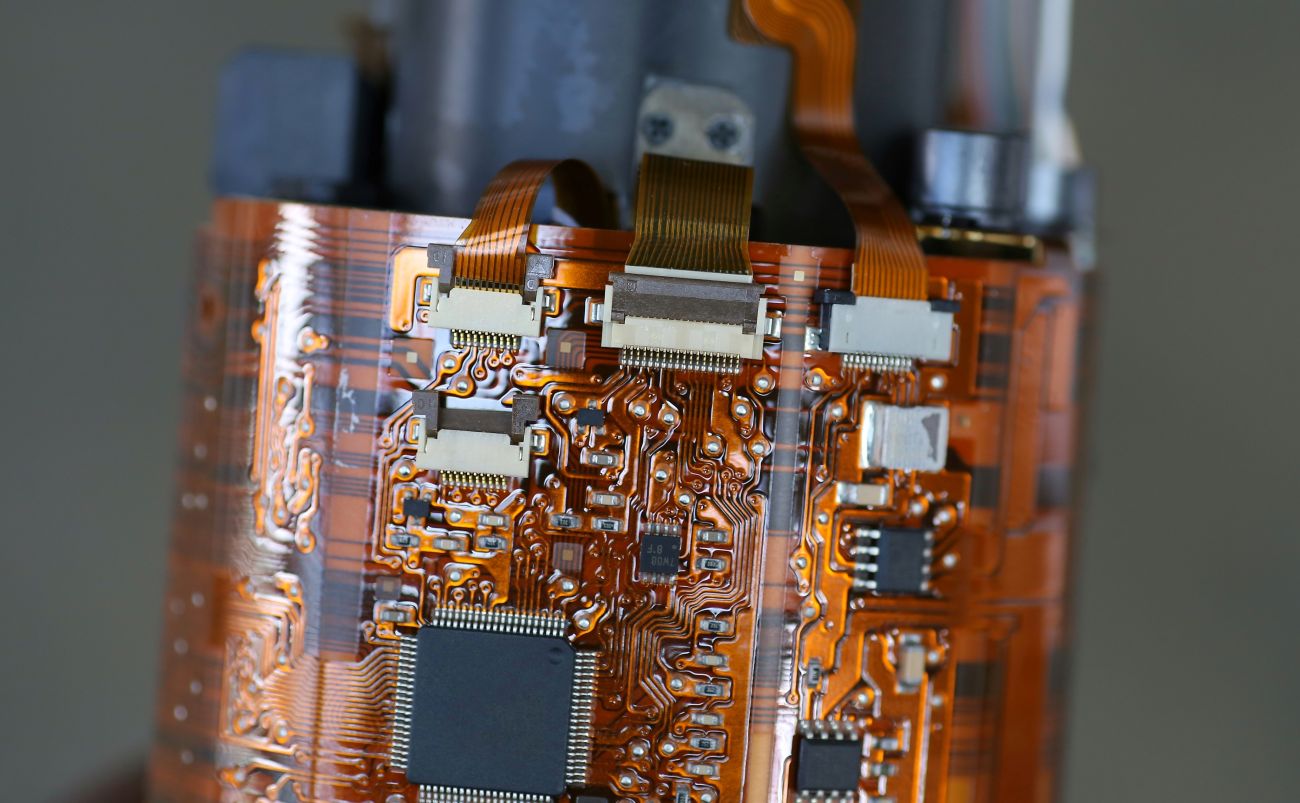
Rigid-flex designs can get very complex very quickly, with multiple layer stacks in the same PCB with rigid and flexible regions. This can make it hard to keep track of things in your CAD system. Fortunately, Altium has an excellent rigid-flex design tool inside the Layer Stack Manager which can help you keep track of all flex and rigid regions.
This guide goes over how to set up the materials, the stack-up regions, and interfaces between different stacks. This includes easy support for stiffeners and rigid-flex sections.
Getting Started in a New PCB Doc File
The first step in a new PCB is to define the layer stack-up. This will be done in a blank PCB doc file in this guide.
Before you start messing around in the Layer Stack Manager in Altium Designer, you should have a plan for what the stack-up will look like. I prefer to draw out an example on paper or in AutoCAD. Within this plan, you can figure out what the flex and rigid regions will look like and where the different layer stacks will be located in the PCB. Starting with a simple 2D drawing, you can then indicate the stack locations by hand.
Now within each of the stacks, think about how many copper layers and rigid layers will be needed. This will be used to set up the individual and common layers inside the Layer Stack Manager. If you can plan this out ahead of time, you can develop a plan for selecting materials in each of the stacks.
Standard vs. Advanced View for Rigid-Flex PCB Stack-Ups
For flex and rigid-flex PCB design, the Layer Stack Manager allows for two different views for creating and arranging materials. These are the standard view, which legacy Altium Designer users should be familiar with, and the newer advanced view which gives a visual representation of the layers in the stack-up. The advanced view is very useful for verification of the layers created in the standard view. However, within the advanced view, you can still create and edit layers which are common to the entire stack or individual to each of the sub-stacks.
Standard Rigid-Flex:

Advanced Rigid-Flex:

I prefer to start creating stacks and materials in the standard view, and then arrange these in the advanced view in order to get a clear visual verification of the layer ordering and common layers. Once inside the advanced view, it is still possible to edit each sub-stack and control whether materials are separate or common to multiple stacks.
Rigid-Flex Stacks or Stiffeners?
As was mentioned above, rigid-flex designs can use an integrated flex ribbon in a rigid section or a stiffener to provide mechanical stability for the design. Both provide mechanical rigidity needed for large numbers of components and fixation or mounting, such as to an enclosure.
Stiffeners: A stiffener is a sheet of pre-preg that is bonded to one side of a rigid-flex board. Components are mounted on the flex side and cannot be mounted on the stiffener side because stiffeners are not laminated with copper. It is possible to drill through stiffeners, but typically drilling is only performed through the flex material. Drilling through allows the creation of a mounting hole as needed.
Integrated Rigid-Flex: This allows additional copper layers to be added to the rigid sub-stack. Fully integrating the flex ribbon into the rigid section allows for double-sided placement of components in the rigid section. Integrated rigid-flex also allows for the formation of blind and buried vias when layer counts get high.
Setting Up Rigid-Flex Design Views
To get started, you will first need to locate the standard and advanced views inside the Layer Stack Manager. The two modes can be accessed from the main menu bar or inside the layer stack design window.

In a new PcbDoc file, there will only be a default layer sub-stack available to use to creat ethe flex/rigid section. Another sub-stack can be created by clicking the “+” button at the top of the layer stack window.

When editing a sub-stack inside the standard view, there is an important checkbox in the properties panel which will enable the flex-only design features. This is the “Is Flex” checkbox; enabling this checkbox is required in order to add flex-only materials, namely adhesives and coverlay layers.
When working in the standard view, it is recommended to follow this workflow:
- Create the flex region first with the “Is Flex” box selected so that the required adhesives and coverlays can be created.
- Add a new sub-stack for a rigid region so that the stiffeners or additional rigid/copper layers can be added.
- Review the layer assignments in the advanced mode
- If there will be multiple bifurcations in the flex ribbon, create a branch and add new substack as required.
The image below shows the correspondence between the standard view and the advanced view for a basic rigid-flex stackup. In the example, the ends of the stackup are integrated rigid-flex regions, and the center is the flex-only region. Inside the standard view (bottom half of the image), we can see the standard view for each sub-stack. Each sub-stack is defined in the standard view by disabling either the flex-specific or rigid-specific materials in the rigid or flex sections, respectively.
The same approach can be implemented with branches in bifurcated rigid-flex designs, such as the example image shown below.
Whether you need to build reliable power electronics or advanced digital systems, use Altium’s complete set of PCB design features and world-class CAD tools. Altium provides the world’s premier electronic product development platform, complete with the industry’s best PCB design tools and cross-disciplinary collaboration features for advanced design teams. Contact an expert at Altium today!

