


Why Future Electronics Designs Might Be Chiplet-Based

At a Glance
Understand why future electronics designs are chiplet‑based. See how AI workloads, yield limits, and packaging drive multi‑die architectures.


Over the past two years, chiplets have evolved from a promising architectural approach to an established one in leading-edge silicon. Major AI accelerators, server processors, and client platforms now use multi-die designs to meet performance, bandwidth, and packaging targets that are increasingly difficult to meet with a single large monolithic die, as demonstrated by NVIDIA’s Blackwell architecture, AMD EPYC 9005, and Intel’s Meteor Lake.
Three forces are behind this shift. First, reticle limits, yield economics, and process-node costs are making it harder to efficiently scale monolithic dies. Second, AI demand has turned these design pressures into an urgent business issue, as hyperscalers need higher compute density, greater memory bandwidth, and tighter coupling between compute and memory. Third, advanced packaging has matured to the point that multi-die integration is practical at a commercial scale through initiatives such as TSMC’s CoWoS and Intel’s advanced process and packaging roadmap.
Designers are now using chiplets to combine compute tiles, I/O dies, and memory in ways that better fit modern AI, HPC, and data center workloads. Standards have advanced, packaging platforms have improved, and shipping products demonstrate that chiplet-based design has arrived.
Key Takeaways
- Chiplets have evolved from a promising architectural approach into production reality in leading-edge AI accelerators, server processors, and high-performance client silicon.
- Three converging forces drove the transition: Moore's Law economics, AI demand, and advanced packaging.
- Standardization through UCIe, FCSA, and OCP is moving chiplets closer to practical multi-vendor interoperability.
- Automotive is emerging as the next major chiplet domain, with the first announced production programs expected in the late 2020s and broader adoption after 2030.
- Multi-vendor mix-and-match integration at scale remains a 2030s story, even as the ecosystem builds toward it.
Chiplet Fundamentals
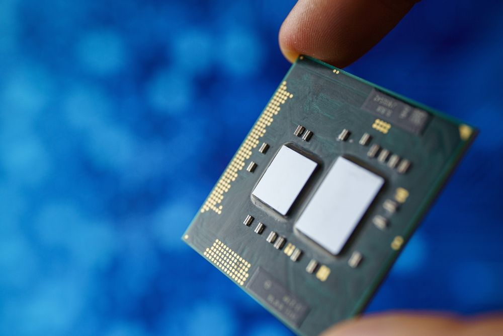
A chiplet is a small, discrete die designed to perform a specific function and then assembled with other chiplets in a single package to form a complete system. Where a traditional monolithic SoC integrates all functions on a single piece of silicon, a chiplet-based design disaggregates those functions into separate dies that communicate via a high-bandwidth die-to-die interconnect.
This modularity offers some compelling engineering advantages. Each chiplet targets the process node best suited to its function: compute-intensive logic on an advanced 3nm or 5nm node, I/O and analog on a mature, cost-effective node where leading-edge lithography adds cost without proportional performance gains. Smaller dies produce better yields, since defect probability scales with die area. And once a chiplet is validated, it becomes reusable IP that can be combined across product families and market segments.
The Three Forcing Functions
- Moore’s Law economics: The extreme ultraviolet (EUV) reticle limits a single die to roughly 858 mm², capping monolithic die size. Defect rates scale with die area, so large dies at advanced nodes carry steep yield penalties. Add mask set costs that can run $30 to $50 million at leading-edge nodes, and the financial case for disaggregation is clear.
- AI demand: Combined hyperscaler capital expenditure on AI infrastructure reached roughly $400 billion in 2025, with Goldman Sachs projecting $1.15 trillion across 2025–2027. This massive investment is driven by training and inference workloads that consume memory bandwidth at a rate monolithic dies cannot satisfy. Chiplet architectures solve this by placing high-bandwidth memory dies adjacent to compute dies on the same interposer.
- Advanced packaging: CoWoS®, Intel’s Foveros 3D stacking, and hybrid bonding have made multi-die integration practical at volume. Die-to-die interconnects now deliver bandwidth densities that approach on-chip levels, removing the performance penalty that once made disaggregation a difficult tradeoff to justify.
Standards Are Catching Up
The engineering case for chiplets was clear before the standards to support them existed. UCIe, the Universal Chiplet Interconnect Express, has improved the situation with a steady release cadence since its 1.0 specification in March 2022. UCIe 2.0 added 3D packaging support and a manageability architecture; UCIe 3.0, released in August 2025, increased data rates to 48 and 64 GT/s and added runtime recalibration for power efficiency. The consortium now counts more than 140 member companies, including AMD, Arm, Google, Intel, Meta, Microsoft, NVIDIA, Qualcomm, Samsung, and TSMC.
In March 2025, Global Unichip Corp. announced the first UCIe PHY silicon on TSMC’s N3P process with CoWoS packaging, achieving 32 Gbps per lane and a bandwidth density of 10 Tbps per millimeter of die edge. This demonstrates that UCIe has moved from specification to silicon-proven IP and public PHY demos.
The open ecosystem is coming together alongside the spec work. The OCP launched the open chiplet marketplace in 2024. In October 2025, Arm contributed the FCSA to OCP, a vendor-neutral specification for partitioning monolithic SoCs into interoperable chiplets across any processor architecture. Together, UCIe, FCSA, and the OCP marketplace form the standardization layer the industry needs for multi-vendor chiplet integration at scale.
Chiplets in Production
AMD’s Instinct MI series and NVIDIA’s Blackwell architecture define the current frontier in AI compute density. The MI300X integrates GPU compute dies and I/O chiplets with HBM3 memory stacks in a single package, and the MI350 series delivers up to 35x faster AI inference than the MI300 generation. NVIDIA’s Blackwell connects two reticle-sized GPU dies with a 10 TB/s chip-to-chip interconnect, a bandwidth figure achievable only through a multi-die architecture.
AMD’s EPYC 9005 series demonstrates that chiplets have moved from differentiator to a standard practice in data center CPUs, combining compute dies with a central I/O die at the heart of current-generation server deployments across cloud and enterprise infrastructure.
Intel’s Core Ultra, which debuted on the Meteor Lake platform in December 2023, is the broadest proof of production viability. Meteor Lake used Foveros 3D packaging to stack compute, graphics, SoC, and I/O tiles, each manufactured on its optimal process node. This volume production of a chiplet-based consumer CPU confirms that chiplet manufacturing has the yield, cost structure, and supply chain depth to support mainstream devices.
Leading players are beginning to collaborate on chiplet technology. For example, in September 2025, NVIDIA and Intel announced a collaboration to develop x86 SoCs that integrate NVIDIA RTX GPU chiplets. An arrangement like this would have been difficult to execute before UCIe and advanced packaging infrastructure were in place.
Automotive: The Next Frontier
The semiconductor pressures that drove chiplet adoption in AI and data center silicon are reaching the automotive sector as well.
Software-defined vehicles demand processing power that grows with each model generation, while automotive product cycles run ten to fifteen years, and safety certification adds qualification overhead that monolithic SoC designs handle poorly at scale. Chiplet architectures address both problems directly: OEMs can upgrade compute performance by swapping chiplets across platforms, reuse already-qualified dies across vehicle lines, and mix process nodes to optimize cost within a single package.
The imec Automotive Chiplet Program, which launched in late 2024, brings together a growing list of partners – including Arm, BMW Group, Bosch, GlobalFoundries, Infineon, Porsche, Siemens, Synopsys, Tenstorrent, and Valeo – focused on developing reference architectures and qualifying interconnect technologies against AEC-Q100 and ISO 26262 requirements.
On the production timeline, Yole Group’s analysis indicates that vehicle designs targeted for 2027 and 2028 production are already locked in, leaving post-2028 as the first realistic window for chiplet integration. Renesas Electronics is among the likely early movers, as one of 12 Japanese semiconductor companies in the Advanced SoC Research for Automotive consortium, targeting chiplet-based SoCs in vehicles from 2030 onward.
In November 2024, Renesas launched the R-Car X5H, its fifth-generation automotive SoC built on TSMC's 3nm process, with support for chiplet extensions that scale AI and graphics performance beyond the base die. Then, at CES 2025, Honda and Renesas announced an agreement to develop a high-performance SoC for Honda's 0 Series EVs, slated for the late 2020s, using the R-Car X5 as the compute foundation extended by an AI accelerator chiplet optimized for Honda's proprietary AI software. These developments are some of the clearest public signals that automotive chiplet integration is moving from roadmap to program.
Remaining Challenges
The path to broad multi-vendor adoption runs through several engineering and ecosystem problems that remain unresolved:
- Known-Good Die testing: Assembling dies that haven't been pre-qualified into a multi-die package increases the risk of package-level yield loss, and rework after assembly is limited. Pre-bond qualification is still maturing as a standardized practice.
- Thermal management: Stacking high-power compute dies, and HBM concentrates heat that traditional cooling struggles with. Microfluidic on-chip cooling shows promise but hasn't reached production scale.
- Security and supply chain trust: Multi-vendor chiplet assembly expands the attack surface and complicates the chain of custody for high-assurance applications. The UCIe Consortium is developing security architecture standards to address this.
- Ecosystem fragmentation: UCIe, OCP’s Bunch of Wires, Arm’s FCSA, and several proprietary interconnect approaches coexist today. True heterogeneous multi-vendor assembly is still more vision than practice.
- Advanced packaging capacity: CoWoS and advanced packaging lines remain in high demand and short supply, creating lead-time and allocation pressures that affect chiplet-based designs.
The Transition Is Underway
Chiplets have evolved well beyond the status of a promising architectural approach. In AI accelerators, server CPUs and high-performance client silicon, they are already a production architecture tied directly to the limits of monolithic scaling and the growing importance of package-level optimization. UCIe, FCSA, and OCP have strengthened the standards picture, while CoWoS, Foveros, and hybrid bonding have made multi-die integration practical at a commercial scale.
Heterogeneous multi-vendor assembly is still maturing, and the standards, supply chain, and tooling will take time to catch up. Even so, the direction is clear. In leading-edge compute, the question today is how quickly the ecosystem can standardize, package, test, and scale chiplet-based systems. The automotive industry is beginning to ask the same question. And with the R-Car X5H platform and the Honda 0 Series program, Renesas is already among the first to build the answer into production silicon.
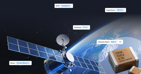
As chiplet‑based systems increase design complexity and supply‑chain dependency, access to accurate component data becomes critical. Explore up-to-date availability, lifecycle status, and sourcing insights across distributors with Octopart →

About Author
Related Resources
Related Technical Documentation
Table of Contents
Design to Release, Without the Friction
- Keep reviews tied to the right version
- Reduce handoff confusion and rework
- Spot sourcing and release risk earlier
- Work solo, share when needed
Get Started
Thank you, you are now subscribed to updates.