
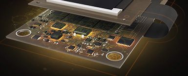


Gaining Insight into Your PCB with Color Displays
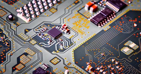
How many PCB design hours have you wasted trying to decipher a legacy project you just inherited? How about wading through thousands of connection lines, trying to determine the best component placement? It can be disheartening, to say the least. What if there was a better way?
How Color Override Can Help You Restructure Designs
Let’s take a look at how you can use Net Color overrides to provide visual enhancements for both the schematic and PCB to give you visual control over your design. Whether you’re creating a new PCB design or reviewing an existing board, you can use the Board Insight Color Override to provide visual assistance for both PCB software and schematic editors.
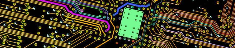
From the very first placement of a wire on your schematic to the first ECO transfer of a design to a PCB layout, Board Insight Colors can be an immediate help for both and the PCB designers. Net Colors are not just the ability to view net connections with an assigned color. Rather, they allow you to see the color display on copper, making your solid layer come alive, with specific colors for ground, power rails, data and address lines. What if there was a way to view these color displays quickly and easily directly in your PCB design software?
Straightforward Board Insight Color Display with Altium Designer
Altium Designer® introduces net color synchronization between schematics and PCB with an efficient color highlighting system. This system allows color assignment in either the schematic or the PCB, as the ECO process keeps them in sync. In the schematic, the net color designation will highlight all wires with the same net as the same color throughout the entire schematic hierarchy. This way, color changes can be made quickly and easily.
Interested in seeing how the tool works within Altium Designer? Download our free whitepaper Breaking the Visual Barrier today for a step-by-step walkthrough in your PCB design software.
About Author
Related Resources
Related Technical Documentation
Table of Contents
Altium is transforming the electronics industry so thoroughly that our web pages need a minute to catch up. For a short time, some information on this page may be outdated.
We appreciate your patience. It will be worth the wait!
Learn More
Thank you, you are now subscribed to updates.