High Voltage PCB Design for Arc Prevention: How to Manage Pads and Traces
Growing up, I’d work obsessively on jigsaw puzzles with my grandmother. Like, skipping dinner obsessively. She was a grandmaster of puzzles; you only got to look at the picture once when you took the pieces out. If you needed more than your memory and pattern recognition, that was cheating. Instead of facing the shame of looking at the box, I learned to focus on the shapes of the pieces, and how each fit with its neighbors. That way, not knowing the exact final picture was less paralyzing.
Laying out traces and pads for a high voltage PCB design reminds me of doing jigsaw puzzles. You have an overall picture in your mind, but the shape of each piece is still important if you want to get the final solution right. There are a couple different aspects to consider for your pads and traces to get the shape just right, especially in high voltage applications.
Best practices for designing corners on your high voltage board
You want to avoid any corners and sharp edges or turns on high voltage Printed Bs. For pads, use a smooth, round curve that cuts off the corners. Design the curve with the largest radius you can without losing the necessary surface area.
When you route the traces, you also want to avoid sharp corners at turns. Instead, use a curved track, again with the largest radius you’ve got space for.
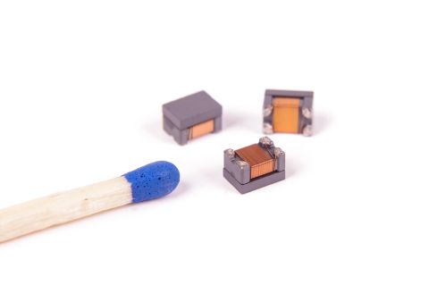
If you are using solder balls at connection points, you should also specify a minimum radius for the solder balls. Make sure you inform your manufacturer before they quote you for the fabrication, since you may need a larger solder ball than they typically use.
Small radius solder balls can concentrate the electric field on a high voltage PCB and increase the risk of arcing or corona events.
Spacing considerations on your high voltage board
By using curved edges instead of corners, you can use much a smaller spacing between features. According to Sierra Proto Board, direct arcing can occur at ⅓ the distance from a needlepoint as compared with a rounded edge. It’s also three times easier for a needlepoint to generate corona.
Sierra Proto also has equations to help you estimate your spacing distance based on your operating frequency. Remember that high frequency will arc more easily, so your spacing increases by a recommended factor of 1.12X.
Once you have your board, make sure that the surface and edges are clean, and all of the conductors are smooth before you power it up. Dirt, rough edges and scratches can all decrease the arc-over voltage by 70-80%
Best practices for designing edges on your high voltage board
Just like edge pieces in a jigsaw puzzle, edges on a Printed Board will need special attention. When the edge of a board is machined or routered, burrs are often left behind on the raw edge. If that happens on a conductive trace, the burr will function like needlepoint and dramatically increase the risk of arcing.
To be safe, your layout should set copper traces back from any edges. Use a minimum buffer distance of 0.02 inches between a conductor and the edge. Increase the distance by 0.001 inches for every 100 V the trace will experience at its maximum load.
Sometimes, you’ve got no choice but to shoehorn a trace in near the edge. In that case, you can use a conformal coat of a high voltage compatible material, like HVPF. The coating allows you to provide additional protection to your PCB out to the edges of the board.
Traces and pads near the edge of a high voltage PCB require special design consideration to protect them from machining damage.
My grandmother will disagree, but mistakes in a Printed Board design are much more serious than mistakes in a jigsaw puzzle. This is why you should make sure that you’re using the best tools possible. An especially helpful feature in design software, like Altium Designer®, is setting your own design rules. That way you don’t have to remember spacing distance and solder ball size while you’re optimizing a layout with only rounded tracks.
Once you’ve put the puzzles away, Live support at Altium is available to help you learn more about how the best PCB software can help you improve your high voltage PCB design process.
Have a question about high voltage PCB design for arc prevention? Contact an expert at Altium.
Check out Altium in action...
PADS® Logic Exporter
Related Resources


Related Technical Documentation

Table of Contents
Take advantage of the world's
most trusted PCB design system.
One interface. One data
model. Endless possibilities.
Effortlessly collaborate with
mechanical designers.
The world's most trusted
PCB design platform
Best in class interactive
routing
View License Options
Thank you, you are now subscribed to updates.