PCB Layout Tip: Save Time with Reusable Blocks

To survive today’s business environment for PCB Designers, design reuse is crucial for quick PCB layout. We must always work faster and smarter. That means whatever available methods might streamline the process to make it more straightforward and faster the better. However, when things go faster, usually more mistakes occur, and they are generally not caught.
One strategy that helps tremendously is using reusable designs. A common practice in other industries is to make reuse of something that works in new designs. For the PCB Designer, this often means going back to an older design and copy and paste. While the practice comes with its inherent problems, there is a better way to do it.
What are Reusable designs?
Reusable Designs is saving a particular design block of either a schematic or the PCB Layout to make reuse in the future. You can save and manage them in a system, on your local computer, or Company server.
Perceived Problems
Design block reuse come with several perceived problems, which often result in not using them at all.
I find that some Electronic Engineers (EE) do not particularly like using reusable designs. I’m not exactly sure why this is the case. However, I have found that many want to design a new product from the ground up. They like testing their design prowess, which does not entirely make sense, since they have a proven and tested previously used design. The primary concern is not prowess but time schedules.
For protection purposes, reusable designs are “Read Only” by their nature. You initially set up reusable design blocks precisely in that previous design, a snapshot we could say. When reused, the designer often wants to make some changes–which makes it no longer a reusable design. With this in mind, they throw out the baby with the bathwater and not use them at all.
To set yourself up for successful design block reuse, you need to know where to break the circuit. You want a circuit that is complete and clear with a limited number of inputs and outputs. The more interconnected inputs and outputs in the reusable block, the more difficult it is to make those connections in the new circuit. These circuits can be of any size; I have seen reusable design blocks with only a couple of components. However, what was very clear was a few input and outputs and self-standing circuit.
So, why don’t we copy and paste a circuit? First, we must find the needed source files (if they still exist) and the specific circuit. All this, I would say, falls under “tribal knowledge,” and maybe very difficult to find if at all.
Also, depending on its age, the circuit might have obsolete components. Unless you check the component sourcing and verify the availability, it could be a significant problem.
What are the types of Reusable Designs in Altium Designer?
Managed Sheets
Managed Sheets are entire designs you save in a controlled environment. These designs can be any size and placed on a schematic template sheet. As an additional benefit, these design should use managed components. In other words, they contain no rogue parts. There are immediate and live component availability information. This way you can handle any sourcing issues immediately.
Managed Sheets are “Read Only.” This means they require several practices including placing all power connections on off-page ports. Place all off-page connections with a Signal Harness and make sure to annotate the design.
Snippets
The second type of reusable blocks is Snippets. These are “Snapshots” of either schematics or the PCB Layout designs. However, Keep in mind that these saved designs are on your local system or company Server.
Snippet best practices include:
-
Always have a central location for your saved snippets. It is best to have this location available to all the designers. Depending on how big your corporation may be, it is best to place them on a Corporate server.
-
Since you can save both the schematic design and the PCB layout, it is best to keep both of those Snippets. In that way, when you use the circuit in a schematic, you can also pull in the PCB Layout Block.
-
Very important when saving a particular Snippet is documenting all the possible details on the circuit in the note area. For example, make sure to include the PCB Snippet place in the PCB Layer Stackup details so you can use the same stackup in the new design.
Design Sheets
The third type of reusable block is Design Sheets. These are very simple to use. You can save an entire schematic sheet in a particular directory and label it as your Design Sheet location. When used they drop into your schematic as a Read Only sheets.
How do reusable designs improve the PCB design and product development process?
-
The first improvement in our design Process is the making of fewer design mistakes. Since these are proven circuits you control in a central location, they are designs you continuously improve as necessary.
-
Another significant improvement is that you can place any information on those reusable design blocks. I have seen some reusable blocks with elaborate info test information, expected signal integrity waveforms and snapshots of datasheets. A significant improvement is the “tribal knowledge” is documented and not lost when particular people leave the company. Whenever you reuse that circuit, all the knowledge comes with it. Those reusable blocks become a useful tool for the designer.
-
Reusable blocks simplifies Multi-Channel Designs. Reusable designs are the backbone of the Multi-Channel features in Altium Designer. When you use a single circuit multiple times, it simplifies the circuit tremendously, especially the number of schematic sheets used. I have seen a reusable block in a Multi-Channel design reduce the schematic down from twenty sheets to only four.
-
Helps in getting through Compliance testing.
When reusable snippets use the PCB Layout primarily, it speeds up any required compliance testing. What is critical is that you take the feedback and update the needed changes in the reusable block. That way you keep improving them.
The bottom line is that reusable design blocks save time. Time truly is money. When we are talking about getting a product to market as quickly as possible, the more advantages you give yourself, the better. When you employ reusable blocks you can make reuse your designs confidently.
With Altium Designer®, you can implement a comprehensive data management strategy that will make reuse old design blocks easy. Would you like to find out more about how Altium can help you with reusing component data on your next PCB design? Talk to an expert at Altium.
About Author
Related Resources


Related Technical Documentation


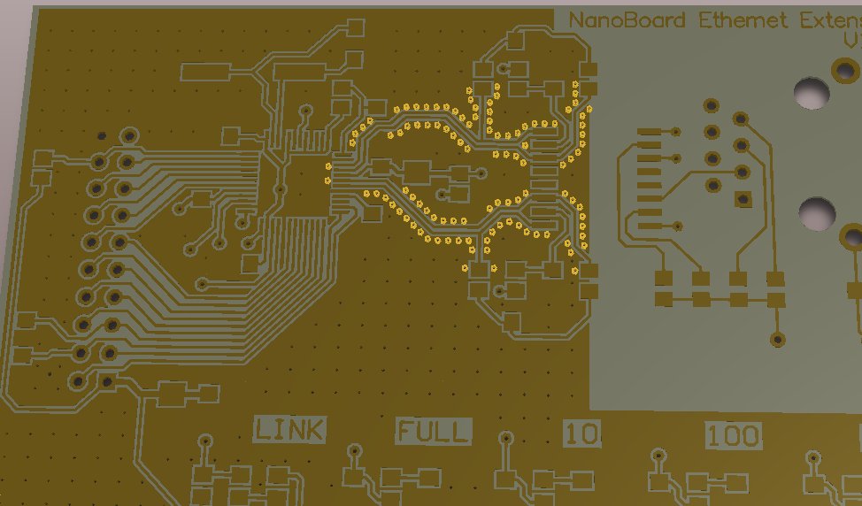


Table of Contents
Take advantage of the world's
most trusted PCB design system.
One interface. One data
model. Endless possibilities.
Effortlessly collaborate with
mechanical designers.
The world's most trusted
PCB design platform
Best in class interactive
routing
View License Options
Thank you, you are now subscribed to updates.