Take the Fear out of PCB Form Factors with These Four Considerations
Throughout the early 2000’s, we were blessed with an array of new and exciting products, shows, music, and technology. Myspace was just coming into view as one of the top social networking sites of its time, Livestrong bracelets were the most fashionable accessories around, and who could forget the launch of the very first iPod. However cool and hip all these things were, there was one that clearly stood out among the rest: the NBC show Fear Factor. OK, maybe it didn’t quite steal the spotlight entirely, but for me and my family Tuesday night Fear Factor was the thing that kept us going. Live bugs, adrenaline pumping stunts, and hair-raising situations; this is what TV was meant to be.
Now that I’m a bit older, the hair-raising situations that I’m finding come from unexpected demands or challenging errors within my PCB designs. Instead of having a fear factor, though, I worry about form factor; there won’t be scorpions crawling across them, and I won’t have to try soldering in a straight line while tarantulas are walking along my shoulders, but considering my PCB design shapes and sizes are a beast to tackle in their own right. But fear not! PCB form factor only requires a bit of forward-thinking, possible with some of these design considerations.
The Smaller the Form Factor, the Larger the Fear Factor
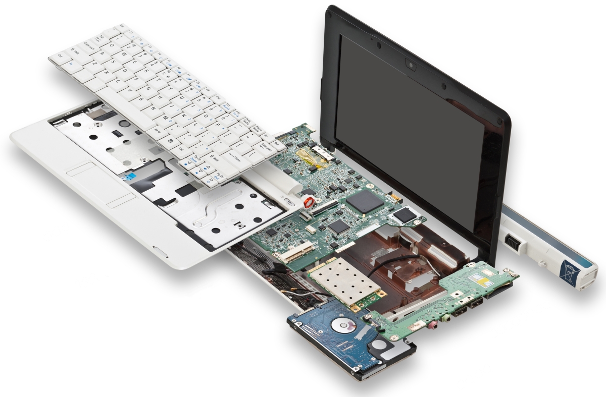
Moving well past the early 2000’s, our iPods are getting smaller, demands are getting bigger, and PCB form factor couldn’t be more of an importance in PCB design. Fitting hundreds of components within smaller and smaller ‘forms’ is certainly cause for heightened fear. And even now, with demands for RF boards and innovations in electronics, a versatile board design has to keep in mind PCB form factor design.
To define: PCB form factor design is an aspect of hardware design which defines the shape, size and other physical properties of a PCB design as a whole. This includes the chassis, internal board configuration, mounting scheme, and so on. With the decrease in the size of PCB devices, and moving further into the small form factor (SFF) arena, there are a handful of considerations to keep in mind to ensure efficiency of your smaller form PCB design throughout the design process.
Design for Assembly
When in your initial stages of your PCB layout, this step is understandably the most overlooked. Early prototyping effort is simply to ensure the design functions and not necessarily the fit and form of the board. Efforts within your design team should be taking all aspects of fit and form into consideration as early as possible so as to keep forward planning as viable of an option for you.
Not only should you require your design team to keep assembly in the back of their mind, but your manufacturing provider should as well. Obviously, you may not be to the point of even considering a manufacturer quite yet, but when you do, ensure that they heavily rely on multiple team interaction. In other words, ensure the design, fabrication, assembly, and procurement teams within the manufacturing plant are in perfect synchronicity with your projects specifications. This will ensure that all problematic areas within the ‘form’ or assembly aspect of the design will be identified early on, saving you many headaches further down the road.
Monitor, Monitor, Monitor
It wouldn’t make sense to cook a Thanksgiving turkey without measuring the temperature at least once, would it? Perhaps you’re feeling lucky though; this is understandable—we all have our bouts of luck. But would you feel the same luck when sending your initial design down the assembly line for the first time? How many times would you think you’d want to test, measure, compare? Placing as many test points along the line as possible under as many variables that could change will ensure segmentation of your PCB form factor issues allowing you to catch mistakes as they happen. This, in turn, will substantially increase your first pass yields.
In addition to keeping an eye on the probe testing throughout the assembly, equipment related tolerances must also be kept in mind. Production machinery inclusive of paste printers, pick and place machines, selective and wave-soldering machines, and the router in charge of the physical cutting (used for board breakout) all have tolerances that may or may not wander. Obviously, these tolerances could wreak havoc on your design when dealing with small form factors. Keeping adequate testing to ensure tolerances are kept in check is never a bad idea.
Panelization Considerations
Arguably the most important aspect when dealing with PCB form factor along your PCB design road is the aspect of panelization. Panelization essentially constructs multiple PCB boards from a single larger board. This saves space, improves the efficiency of assembly, and saves loads of time and money compared to assembling one board at a time.
Keeping tolerances in mind like whether you choose a V-groove or perforated breakout design may make or literally break your design. Edge clearance comes into play here more than ever, and when dealing with a smaller and smaller form PCB, you will need to ensure proper clearance values to avoid breakout flaws.
Ducks and Documentation: Keeping Them Both in a Line
Keeping your levels of documentation in sync should be extremely high on the priority list when closing in on your production goals. Losing sight of various design changes along the way will leave you disoriented and at a loss for time when trying to find your way back around. Hierarchical design, component and data management, and a unified platform for tracking changes will all be essential when entering into the later stages of design.
As amazing as the early 2000’s may have been for some, we are certainly far past the days of jamming out to NSync, rolling down the sidewalk in our Heelys, and the unfortunate and inevitable burn out from Fear Factor. However, now that we can confidently go about mitigating PCB form factor design issues within the PCB process, our factor of fear will burn out just the same leaving us free and clear to focus on what we as PCB design engineers do best; design awesome PCBs!
There are a plethora of helpful products and features within Altium Designer® that will assist in nearly every PCB form factor design capacity. These include schematic capture capabilities, component management, board layout, and the list goes on.
If you would like to discuss your specific smaller form PCB related issues or if you have other form factor design questions, talk to an Altium expert today!


