Oscillations, Clipping, and Ringing in Amplifier Stability Analysis


Op amps probably form the basis of amplifier knowledge for many digital designers, and there may not be much that comes after that in electronics classes. A friend of mine once joked, “you only needed to learn RF and analog circuits to pass your qualifying exams.” This is understandable; unless someone has worked in telecom or developing test instruments, they probably worked mostly on low frequency analog or in digital systems and did not have much need for high frequency amplifier circuits. Nowadays, more systems are integrating analog circuitry alongside digital at high frequencies (e.g., wireless on IIoT products), creating a need for on-board amplification.
One aspect of amplifiers that is sometimes poorly discussed in component datasheets is the possibility of instability in the output from an amplifier. I discussed the possibility for RF amplifier instability in an earlier article due to unintended feedback from parasitic capacitance, but instabilities can also happen at lower frequencies where parasitics may not be the main culprit. Let’s look at what causes these instabilities and how to use some simple amplifier stability analysis calculations to better understand your amplifiers.
What to Watch for in Amplifier Stability Analysis
There are three primary instability effects that occur in amplifier circuits:
- Clipping: When driven too high with negative feedback, or when positive feedback dominates, the amplifier can saturate and will clip. This is due to the inherent nonlinear behavior and feedback in all amplifier circuits.
- Ringing: This appears as an underdamped oscillation, normally when the amplifier is driven with a step input. In other words, this is a transient response in the output signal matching what would occur in an underdamped RLC circuit.
- Oscillations: This effect is exactly as it sounds: the output oscillates with some definite frequency. This may be intentional (e.g., in a multivibrator circuit) or unintentional (when driven periodically around a pole).

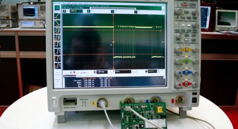
The above graph shows examples of ringing and clipping; note that ringing and oscillations are related in that oscillations can occur without damping. Let’s look at each of these areas in greater depth to see what can be done to prevent these problems at the schematic level and board level.
Ringing and Oscillations
Ringing and oscillations are related in that the former is a transient effect and the latter is a driven effect, and both are determined by poles in the circuit. Both of these effects are caused by driving a capacitive load and due to some phase shift in the amplifier’s feedback loop. All integrated circuits and discrete components have some input capacitance (a parasitic shunt capacitance to the nearest ground plane). This creates some phase lag in the feedback loop.
In the simplest model, the load capacitance adds a single pole to the amplifier’s open loop gain (assumes infinite load input impedance and nonzero amplifier output inductance). As a result, the real loop gain in a negative feedback amplifier is frequency-dependent, but no longer follows the simple relationship given by the gain-bandwidth product. This is shown below:

The above circuit produces gain with a non-inverted output, but this can be multiplied by -1 for an inverted output. In either case, the goal is to prevent the inputs at the inverting and non-inverting inputs from being perfectly out of phase, as they will then become additive; pay attention to the phase margin specification in your datasheets. This is where the two feedback impedances become very important as the equation above can be used to tailor the phase shift in the feedback loop to a specific value. Some options for modifying the feedback loop to prevent ringing in an amplifier’s output include:
- Adding a series resistor on the output to increase damping (out-of-the-loop compensation)
- Adding a feedback capacitor as a parallel feedback loop to modify the feedback phase shift (in-the-loop-compensation)
- For rail-to-rail amplifiers, shunt the oscillation to ground with a series RC circuit (snubber network)
Persistent oscillations can also appear due to unintentional coupling back to the non-inverting input for sufficiently high gain values, input signal levels/frequencies, and levels of capacitive coupling. Whether oscillations appear as ringing or continuous oscillations, the exact solution needed to compensate your amplifier depends on the amplifier’s construction, output impedance, and linear transfer function. Make sure you use the right amplifier component model in your schematics when running SPICE simulations for your circuits.
Clipping
Clipping is generally undesirable unless you’re building something like a comparator, which actually exploits positive feedback and hysteresis to create a saturated output. For clipping, there is nothing you can do at the circuit level unless you’re designing a multichain amplifier for your signal chain. In that case, make sure successive stages are not saturating each other; this is a more complicated topic that deserves its own technical article. The other option is to bring up the rail voltage and increase your available power at the supply if you really need to get to such high output voltages.
In the extreme case, where there is strong unintentional coupling between the output and the inputs, there can be some clipping. This can occur at very high input powers, e.g., in an RF power amplifier, and at very high frequencies (e.g., mmWave amplifiers). As was detailed in the earlier article on amplifier stability, the solution is to properly layout the amplifier on the PCB so that parasitic coupling is reduced. I’ll discuss this more in a future article as it is an in-depth topic.
K-factor from S-parameters
There is one factor that many application notes on amplifier stability analysis do not mention: the K-factor, originally formulated in John Rollett's 1962 IEEE paper entitled Stability and Power-Gain Invariants of Linear Twoports. If you can calculate the S-parameters for your amplifier circuit in the linear regime, you can use the following K-factor definition to immediately see whether the amplifier will be stable:

In short, the amplifier will be unconditionally stable when K > 1. If this condition is not satisfied, then you might have an unstable amplifier, and you should do more simulations to determine whether your amplifier design is really unstable and in which situations instability arises. Like many cases in circuit design and PCB layout, a system can be unstable, but the instability can be so minor that it goes unnoticed and never interferes with system operation. In other cases, you’ll need to carefully compensate capacitive loading as described above to ensure your design is stable.
If you’re designing an amplification stage for an analog board and you need to use simulations for amplifier stability analysis, the circuit design and layout tools in Altium Designer® can help you optimize your design to prevent oscillations. You can import simulation models for real components, define in your drill table and fabrication documents, and prepare all other deliverables for manufacturing.
When you’ve finished your design, and you want to share your project, the Altium 365™ platform makes it easy to collaborate with other designers. We have only scratched the surface of what is possible to do with Altium Designer on Altium 365. You can check the product page for a more in-depth feature description or one of the On-Demand Webinars.


