Create high-quality PCB designs with robust layout tools that ensure signal integrity, manufacturability, and compliance with industry standards.
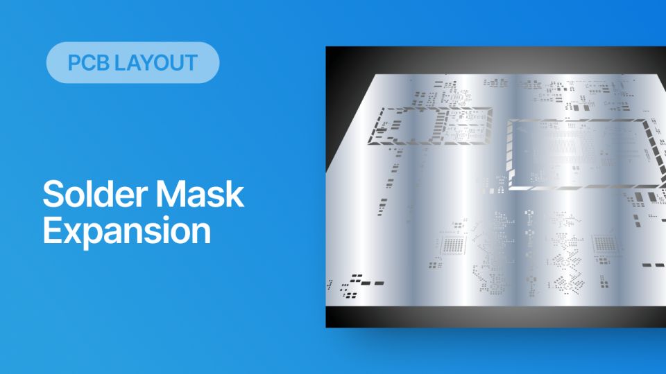
The solder stop mask layer caps off the PCB and provides a protective film over copper on the surface layers
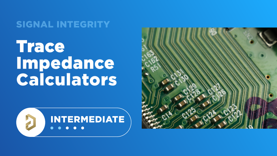
We’ve compiled a set of transmission line impedance calculators for use in high speed PCB design and RF design.
The electronics supply chain is seeing record investment, yet engineers are still projecting longer lead times and higher prices for components.
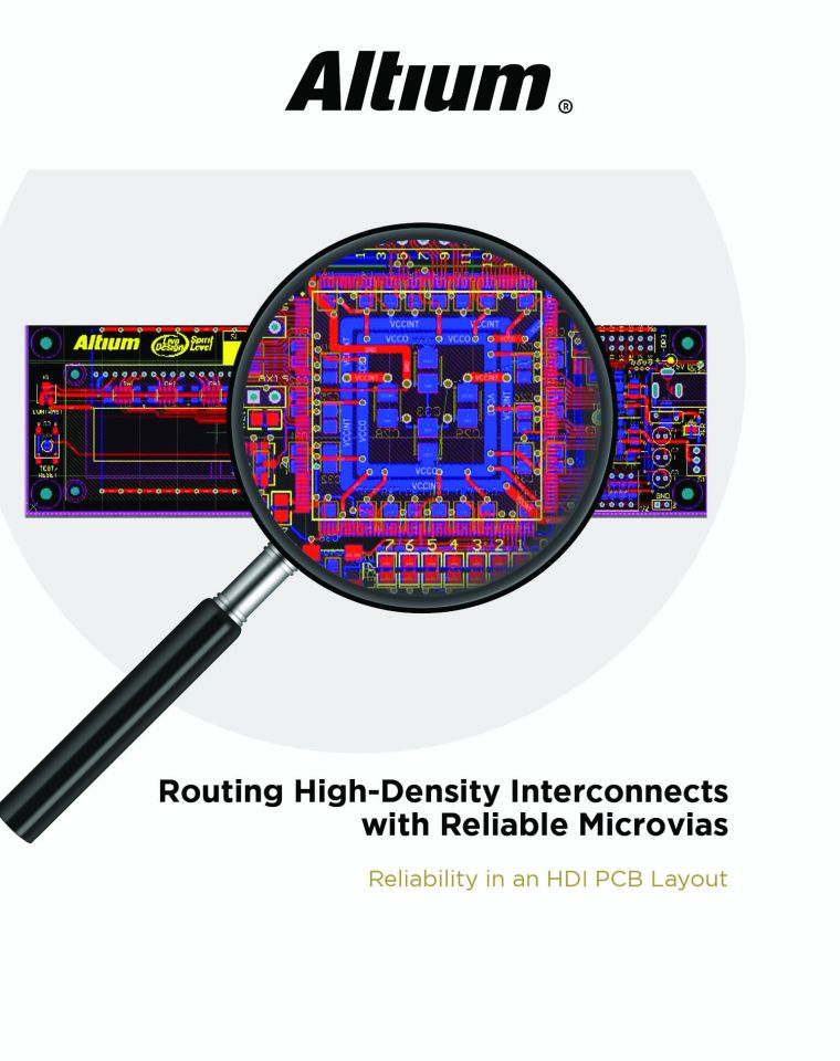
Routing high density PCBs is heavily rules driven and it requires understanding what contributes to microvia reliability.
February 18, 2022 ONTRACK BI-WEEKLY The newest release of Altium Designer brings users new supply chain insights, DFM features, and
Learn how to reduce parasitic capacitance so you can prevent high-frequency noise coupling in your PCB layout.
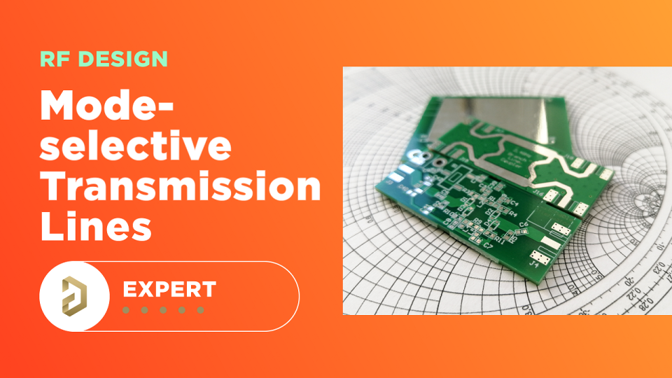
High frequency and data rate channels can be routed as a mode-selective transmission line. Here’s when you should consider this routing technique.