


Introduction to Flex PCB Materials

At a Glance
Learn how to properly select flex PCB materials for accommodating rigid-flex designs and how choosing the right flex circuit materials helps mitigate field failures.


Flex PCB materials need to support multiple design and operational goals: static or dynamic flexing, the ability to pass through standard assembly processes, and support for simple fabrication procedures with high yield. Flex PCB materials may seem exotic at first, but a relatively small material set is used to produce flex and rigid-flex PCBs at high volume. In this guide, we'll examine some of the basic properties of flex PCB materials and how they are used to build flex/rigid-flex PCBs.
Substrate and Coverlay Films
The base material used in most common rigid printed circuit boards is woven fiberglass impregnated in epoxy resin. It’s a fabric, and although we term these “rigid” if you take a single laminate layer they have a reasonable amount of elasticity. It’s the cured epoxy that makes the board more rigid. Because of the use of epoxy resins, they are often referred to as organic rigid printed circuit boards. This is not flexible enough for many applications though for simple assemblies where there’s not going to be constant movement it can be suitable.
The most common material choice used as a flex PCB substrate is polyimide. This material is very flexible, very tough, and incredibly heat resistant.

Flexible Polyimide film (source: Shinmax Technology Ltd.)
For the majority of flex circuit applications, more flexible plastic than the usual network epoxy resin is needed. The most common choice is polyimide, because it’s very flexible, very tough (you can’t tear or noticeably stretch it by hand, making it tolerant of product assembly processes), and also incredibly heat resistant. This makes it highly tolerant of multiple solder reflow cycles, and reasonably stable in expansion and contraction due to temperature fluctuations.
Polyester (PET) is another commonly used flex-circuit material, but it’s not tolerant enough of high temperatures to survive soldering. I have seen this used in very low-cost electronics where the flexible part had printed conductors (where the PET could not handle the heat of lamination), and needless to say nothing was soldered to it - rather, contact was made by crude pressure with an isotropic conductive elastomer.
The display in the product in question (a clock radio) never really worked too well due to the low quality of the flex circuit connection. So for rigid-flex, we’ll assume we’re sticking to the PI film. (Other materials are available but not often used).
PI and PET films, as well as thin flexible-epoxy-and-glass-fiber cores, form common substrates for flex circuits. The circuits must then use additional films (usually PI or PET, sometimes flexible solder mask ink) for coverlay. Coverlay insulates the outer surface conductors and protects from corrosion and damage, in the same way a solder mask does on the rigid board. Thicknesses of PI and PET films range from ⅓ mil to 3 mils, with 1 or 2 mils being typical. Glass fiber and epoxy substrates are sensibly thicker, ranging from 2 mils to 4 mils.
Conductors
While the above-mentioned cheap electronics may use printed conductors - usually some kind of carbon film or silver based ink - copper is the most typical conductor of choice. Depending upon the application different forms of copper need to be considered. If you are simply using the flexible part of the circuit to reduce manufacturing time and costs by removing cabling and connectors, then the usual laminated copper foil (Electro-Deposited, or ED) for rigid board use is fine. This may also be used where heavier copper weights are desired to keep high-current carrying conductors to the minimum viable width, as in planar inductors.
But copper is also infamous for work-hardening and fatigue. If your final application involves repeated creasing or movement of the flex circuit you need to consider higher-grade Rolled Annealed (RA) foils. The added step of annealing the foil adds to the cost considerably. But the annealed copper can stretch more before fatigue cracking occurs and is springier in the Z deflection direction - exactly what you want for a flex circuit that will be bending or rolling all the time. This is because the rolling annealing process elongates the grain structure in the planar direction.
If you are simply using the flexible part of the circuit to reduce manufacturing time and costs by removing cabling and connectors, then the usual laminated copper foil for rigid board use is fine.

Exaggerated illustration showing the annealing process applied to flex PCB materials, obviously not to scale. The copper foil passes between high-pressure rollers which elongate the grain structure in a planar orientation, making the copper much more flexible and springy than normal.
Adhesives
Traditionally, adhesives are required for bonding the copper foil to PI (or other) films, because, unlike a typical FR-4 rigid board, there’s less “tooth” in the annealed copper, and heat & pressure alone is not enough to form a reliable bond. Manufacturers offer pre-laminated single- and double-sided copper-clad films for flexible circuit etching, using acrylic or epoxy-based adhesives with typical thicknesses of ½ and 1 mil. The adhesives are specially developed for flexibility.
“Adhesiveless” laminates are becoming more prevalent due to newer processes that involve copper plating or deposition directly onto the PI film. These films are chosen when finer pitches and smaller vias are needed as in HDI circuits.
Silicones, hot-melt glues, and epoxy resins are also used when protective beads are added to the flex-to-rigid joins or interfaces (i.e. where the flexible part of the layer stack leaves the rigid part). These offer mechanical reinforcement to the fulcrum of the flex-to-rigid join which otherwise would rapidly fatigue and crack or tear in repeated use.
Single Layer Flex Circuits
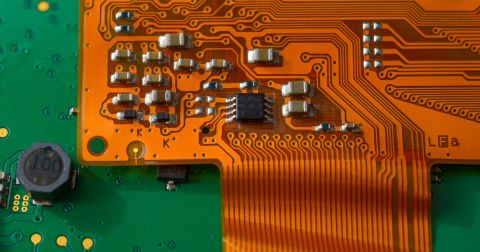
An example of a typical single-layer flex circuit cutaway view is illustrated below. This is the same construction used for most common off-the-shelf FFC (Flexible Flat Connector) cables, which are an alternative to using rigid-flex PCBs where FFC connectors can be accommodated and cost is the primary factor driving design decisions. In single-layer flex circuits, the copper is pre-laminated onto the PI film by the material vendor, then the copper is etched and drilled with a rigid backing plate. This is finally laminated with an adhesive-based PolyImide coverlay that is pre-punched to expose the copper pads. The adhesives used in this arrangement for coverlay can squeeze out in the process, but this can be accommodated by enlarging the pads in the exposed areas.

Typical single-layer Flex Circuit stack-up.
It’s important to be aware of the materials used in flexible and rigid-flex circuits. Even though you may generally give a fabricator freedom to select the materials to ensure yield, you should remain aware of the factors that can cause a flex PCB to fail in the field. Knowing the material properties will also help in the mechanical design, evaluation, and testing of your product. If you are working on automotive products for instance; heat, moisture, chemicals, shock & vibration - all need to be modeled with accurate material properties to determine the product’s reliability and minimum allowed bending radius. The irony is that the driving needs that cause you to choose flexible and rigid-flex are often tied to harsh environments. For example, low-cost consumer personal electronic devices are often subjected to vibrations, dropping, sweat, and worse.
One great resource with far more detail than the introduction shown in this article can be found in Coombs' 2008 textbook:
- Coombs, C. F. (Editor, 2008) The Printed Circuits Handbook, 7th Ed. 2008 McGraw Hill.
Stackup Example
Just like in rigid PCBs, flex PCBs and rigid-flex PCBs can have complex stack-ups as more conductive layers are added. These stacks can involve multiple flex sections in the same PCB, such as in the example shown below. For a pure flex circuit (as opposed to rigid-flex) the layer stack planning is simplified, including in each section of the PCB. However, there may still be points requiring the placement of stiffeners in areas where components are mounted or where the circuit is terminated.

In your design software, each of these sections is defined as its stack and applied to different regions in the PCB layout. When it's time to manufacture the board, each board section will need to be clearly shown in fabrication drawings to illustrate the layer arrangement and materials in the board. We'll discuss this important aspect of flex design and production in a later section.
When you're ready to select and specify the flex PCB materials you need, use the complete set of CAD features and automated drawing tools in the Draftsman package inside Altium Designer®. Once you're ready to release your design data to your manufacturer, you can easily share and collaborate on your designs through the Altium 365™ platform. Everything you need to design and produce advanced electronics can be found in one software package.
We have only scratched the surface of what is possible to do with Altium Designer on Altium 365. Start your free trial of Altium Designer + Altium 365 today.
About Author
Related Resources
Related Technical Documentation
Table of Contents
Design to Release, Without the Friction
- Keep reviews tied to the right version
- Reduce handoff confusion and rework
- Spot sourcing and release risk earlier
- Work solo, share when needed
Get Started
Thank you, you are now subscribed to updates.

