


The Rigid-Flex PCB Manufacturing and Fabrication Process

At a Glance
Learn how to navigate the rigid-flex PCB fabrication process. By knowing the fabrication process, you'll have assurance you can hit yield and performance targets.


If you thought the rigid PCB fabrication process was complex, then flex PCB manufacturing might seem to be on another level of complexity. However, many of the same steps used in standard rigid board fabrication conceptually transfer flex PCB fabrication. This guide provides an overview of all the steps implemented in the flex PCB manufacturing process. These processes are very similar to rigid PCB fabrication processes but involve different material sets as illustrated in an earlier guide.
Flex Build-Ups
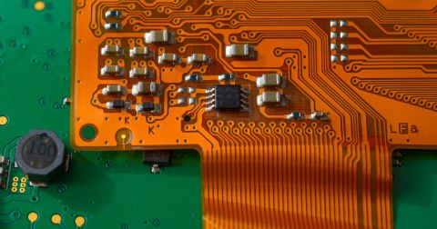
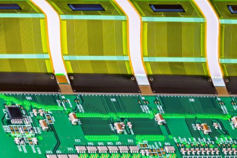
At first glance, a typical flex, or rigid-flex board, looks straightforward. However, the nature of these requires several additional steps in the build-up process. The rigid-flex board fabrication process involves multiple steps like material preparation, drilling, plating, etching, and stripping.
The beginning of any rigid-flex board is always the single or double-sided flex layers. The fabricator may begin with pre-laminated flex with foil or may begin with unclad PI film, and then laminate or plate up the copper for the initial cladding. Laminating the film requires a thin layer of adhesive, whereas adhesiveless cladding requires a “seed” layer of copper. This seed layer is initially planted using vapor deposition techniques (i.e. sputtering), and provides the key to which chemically deposited copper is plated. This one or two-sided flex circuit is drilled, plated through, and etched in much the same steps as typical 2-sided cores in rigid boards.
Flex Fab Steps
The steps below show Flex-Circuit creation for a typical double-sided flex circuit.
Step 1: Adhesive/Seed coating applied

An epoxy or acrylic adhesive is applied, or sputtering is used to create a thin copper layer for a plating key.
Step 2: Copper foil added

Copper foil is added either by lamination to the adhesive (the more mainstream approach) or chemical plating onto the seed layer. Newer fabrication processes by materials vendors allow adhesiveless lamination of rolled annealed copper as an alternative.
Step 3: Drilling

Holes to vias and pads are most often mechanically drilled. Multiple plated flex substrates can be drilled simultaneously by combining them from multiple reels on drums, drilling between work plates, and then rolling out to separate reels on the other side of the drilling machine. Pre-cut flex panels can be combined and drilled between rigid blanks in the same way rigid cores are drilled as well, though it requires more careful registration, and the alignment accuracy is reduced. For ultra-small holes, laser drilling is available, though at a much-added cost because each film has to be drilled separately. This would use Excimer (ultraviolet) or YAG (Infrared) lasers for higher accuracy (microvias), and CO2 lasers for medium holes (4+ mils). Large holes and cutouts are punched, but this is a separate process step.
Step 4: Through-hole plating

Once the holes are made, copper is deposited and chemically plated in the same way as rigid PCB cores (commonly referred to as Cuposit). Through-hole plating in flex circuits should be at least 1 mil in plating thickness to add mechanical support to the pad or via, whereas a typical low-cost rigid PCB may only have ½ mil composite.
Step 5: Etch-resist printing

A photosensitive etch resist is coated onto the film surfaces, and the desired mask pattern is used to expose and develop the resist before the chemical etching of the copper.
Step 6: Etching and stripping

After exposed copper is etched, the etch resist is chemically stripped from the flex circuit.
Step 7: Coverlay or Covercoat

The top and bottom areas of the flex circuit are protected by coverlay layers which are cut to shape. There may be components mounted on sections of the flexible circuit, in which case the coverlay is also acting as a solder mask. The most common coverlay material is additional polyimide film with adhesive, though adhesive-less processes are available. In the adhesive-less process, a photo-imageable solder mask (the same as used on rigid board sections) is used, essentially printing the coverlay onto the flex circuit. For coarser cheaper designs screen printing is also an option with the final curing of this covercoat film by UV exposure. The difference is that coverlay is a laminated film, whereas covercoat is an applied material coating that then needs to be cured.
Step 8: Cutting out the flex
The final step in creating the flex circuit is cutting it out. This is often referred to as “blanking”. The high-volume cost-effective blanking approach involves a hydraulic punch and die set, which involves reasonably high tooling costs. However, this method allows punching out of many flex circuits at the same time. For prototype and low-volume runs, a blanking knife is used. The blanking knife is a long razor blade, bent into the shape of the flex circuit outline and affixed into a routed slot in a backing board (MDF, plywood, or thick plastic such as Teflon). The flex circuits are then pressed into the blanking knife to be cut out.
Lamination and Routing
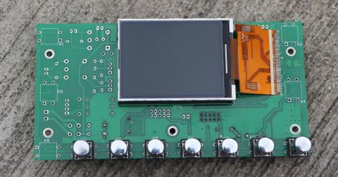
If the flex circuit is to form a part of a rigid/flex combined stack-up (which is what we are interested in), the process doesn’t stop there. We now have a flex circuit that needs to be laminated in between the rigid sections. This is the same as an individual drilled, plated, and etched core layer pair, only much thinner and more flexible due to the lack of glass fiber. As noted previously though, a less flexible layer could be made with PI and glass depending on the target application. Because this is being laminated in between rigid sections, it ultimately has to be framed in a panel that mates with the rigid board panel sections as well. Flex circuits that are not being combined with rigid sections are adhered temporarily to a rigid backing board of MDF or FR-4 style materials.

How the etched, plated, coverlayed, and blanked flex panels are combined with the glass-epoxy rigid panels.
The flex circuit is laminated into the panel along with the rigid and any other flexible sections, with additional adhesive, heat, and pressure. Multiple flex sections are not laminated adjacent to each other unless you are designing multi-layer flex. This generally means each flex section has a maximum copper layer count of 2 so flexibility is maintained. These flex sections are separated by rigid pre-pregs and cores or PI bonding sheets with epoxy or acrylic adhesives.
Essentially, each rigid panel is separately routed out in the areas where the flex is going to be allowed to, well, flex. Here is an example process of laminating into a rigid-flex board, with two, 2-layer flex circuits embedded between three rigid sections. The layer stack-up would look like that shown below.
Note: Many designers are shying away from using adhesives, due to unacceptable z-axis expansion during reflow soldering.

Detailed Stack Diagram including plated-through holes for each flex section, as well as final through-plated holes in the rigid section.
In the example stack-up shown above, we have two pre-etched and cut flex circuits, each double-sided and plated through. The flex circuit has been blanked into a final assembly panel including borders for framing - this will keep the flex circuit flat during final assembly after lamination with the rigid panel sections. There are certainly some potential hazards with inadequate support of flex circuit elbows and large open sections during assembly - especially in the heat of a reflow oven.
While this example does show adhesive layers it’s important to note that many designers are shying away from using adhesives, due to unacceptable z-axis expansion in reflow. However, FR-4 prepreg and thermosetting epoxies effectively achieve the desired result and are here considered ‘adhesive’ layers. Additional adhesion can be achieved through treatment of the copper on the flex layers to improve the ‘tooth’ into the laminated prepregs. Adhesiveless double-sided flex laminates are shown here. These are entirely polyimide films with a bondable polyimide coating which the copper foil is bonded to. DuPont™ Pyralux® and Rogers Corp. R/Flex® are examples of popular adhesiveless laminates.
The coverlay is also applied - like stickers laminated on with adhesive, or by a photo-printing process as mentioned earlier. Once the final flex and rigid panels in this 6-layer stackup are placed together, they are laminated with the outermost (top and bottom) final copper foil layers. Then another drilling for top-to-bottom plated through holes is done. Optionally, laser-drilled blind vias (top to first flex, bottom to last flex) could also be made, again adding expense to the design. The holes are plated through from top to bottom, and blind vias if there are any, and the final outer layer of copper patterns are etched. The final steps are the printing of the top and bottom solder mask, top and bottom silkscreen, and preservative plating (such as ENIG) or hot air leveling (HASL).
Whether you need to build reliable power electronics or advanced digital systems, Altium Develop unites every discipline into one collaborative force. Free from silos. Free from limits. It’s where engineers, designers, and innovators work together as one to create without constraints. Experience Altium Develop today!
About Author
Related Resources
Related Technical Documentation
Table of Contents
Design to Release, Without the Friction
- Keep reviews tied to the right version
- Reduce handoff confusion and rework
- Spot sourcing and release risk earlier
- Work solo, share when needed
Get Started
Thank you, you are now subscribed to updates.


