Mobile menu
PCB Design
Altium Designer
World’s Most Popular PCB Design Software
CircuitStudio
Entry Level, Professional PCB Design Tool
CircuitMaker
Free PCB design for makers, open source and non-profits
Why Switch to Altium
See why and how to switch to Altium from other PCB design tools
Solutions
For Enterprise
The Last Mile of Digital Transformation
For Parts and Data
Extensive, Easy-to-Use Search Engine for Electronic Parts
Altium 365
Resources & Support
Explore Products
Free Trials
Downloads
Extensions
Free Altium 365 Tools
Online PCB Viewer
Resources & Support
Altium / Renesas Scheme: Information for Shareholders
All Resources
Support Center
Documentation
Altium Community
Forum
Bug Crunch
Ideas
Education Programs
Professional Training / Certification
University / College Educators
University / College Students
Webinars
Store
Search Open
Search
Search Close
Sign In
Schematic Capture
Main menu
Home
PCB Design
Collaboration
Component Creation
Data Management
Design Outputs
ECAD/MCAD
HDI Design
High Speed Design
Multi-Board
PCB Layout
PCB Routing
PCB Supply Chain
Power Integrity
RF Design
Rigid Flex
Schematic Capture
Signal Integrity
Simulation
Software
Altium 365
Altium Designer
Enterprise Solutions
PDN Analyzer
Upverter
Education
Programs
Altium Academy
Engineering News
Guide Books
Newsletters
Podcasts
Projects
Training Courses
Webinars
Whitepapers
FREE TRIALS
Unparalleled Schematic Capture
Easily design schematics of any complexity.
Learn More
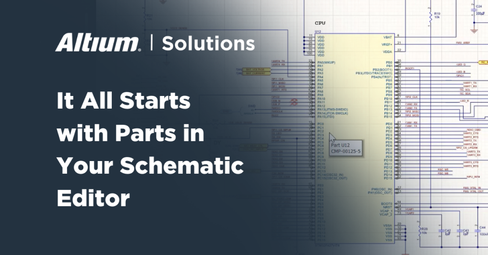
Schematic Capture and Schematic Entry
Eliminate Mistakes in Your Schematics with Electronic Rule Checking
In times of rising design complexity and shortened timelines, it’s more and more for mistakes to sneak through in the schematic that can translate to the printed circuit board. Read on to find out how to easily identify and eliminate issues in your schematic with the Electronic Rule Checking your PCB in Altium Designer
®
. Many designers and companies put all their efforts in having a proper PCB layout and, nowadays, checking in real time the
Read Article
Isolate Objects on a Design with Custom PCB Queries
It can be a great challenge for engineers to make edits to specific objects on overpopulated boards. Leverage the global editing and custom query features in Altium Designer
®
to easily locate objects and maintain consistency in your designs. Read on to learn more. Every faces significant challenges once a board gets overpopulated with and traces. One of the greatest tasks of working with complex electronic designs is managing a large number of
Read Article
The PCB Design Guide for Engineers Part 2 - PCB Planning
As a PCB designer, the planning of the development of a one or several printed circuit boards can be a daunting task. There will be a host of other software tools that will be used in the development of your project. From tools that can be used to track the progress of your human resources within your team to the software tools used by your internal and external resources to bring your project to life. What about high speed components, the solder
Read Article
Experience a Completely Unified Design Environment
With today’s ever growing market expectations, strict project deadlines, and increasingly complex designs, what solutions exist to minimize the time spent switching between your design tools to complete projects? Now you can successfully deliver products on time and within budget in a completely unified design environment. Read on to find out how. Do you feel like your schematic and pcb tools are from different planets? Are you still using a
Read Article
PCB Design Variant Management to Synchronize Designs
Product customization is increasingly popular to satisfy customer demand as both time-to-market and the complexity of products continue upward without abatement. By making variations of a baseline product, the new products can address different markets and requirements. But how do you go about keeping synchronized PCB variants? Making the Case for PCB Design Variants You are developing a PCB layout for a smartwatch that comes in three different
Read Article
Synced Up Designs: Syncing Your Schematics and PCB Layouts Increases Efficiency and On-Time Delivery
A while back, I was working at a company that designs and installs systems for automating smart irrigation and environmental monitoring. We had gotten into the habit of making last minute “hacks” (pin swapping, gate swapping, etc.) to our boards to accommodate a specific need from a job (or to compensate for a design flaw or oversight on a particular model after getting it back from the manufacturer). While this improvisatory method worked in the
Read Article
PCB Design Guide for Engineers: Part 2 — Planning
PCB Design Guide for Engineers Part 2 - Planning The PCB Design Guide for Engineers is a series that serves as a guide for the novice/student, or electronics engineering professional. It presents a description of the methods, stages, and practices in producing a PCB from an engineer’s vision. From conception to delivery of the fully assembled PCB, this document takes you through basic design stages along with giving you proven industry practices
Read Article
PCB Design Guide for Engineers: Part 1 The Team
INTRODUCTION What people are involved in the PCB design & engineering process? Surely all of the tasks of creating a PCB layout don’t just fall on single pair of shoulders. There are many engineering and scientific disciplines that must be harnessed and managed to bring your vision to life. As the project engineer, your first task is identifying your team. PCB Design Guide for Engineers Part 1: The Team This PCB Design Guide for Engineers: Part 1
Read Article
Unleash Your Creativity — With Training
Learn how to use neck-downs in Altium Designer to simplify your BGA routing process by shrinking and expanding tracks as they enter specific areas on your PCB. When you train decreases your errors range and expand your creative capacity. And this get better when you do the right choice selecting able people to training. Beyond that, the personal satisfaction of creating better, more reliable products is just plain fun! After all, didn’t you
Read Article
5 Ways to Customize Altium Designer for Better Efficiency
The Altium Designer
®
environment is designed to be very intuitive, but even slight customization of the interface can greatly enhance the efficiency of your PCB design workflow. Once you have been using Altium Designer or a while, you'll find the toolbar menu structure to be very intuitive. However, you may realize even more productivity gains with customization of the user interface. Customization is centric to each editor whether it's the
Read Article
Quickly Create Project Libraries from the Schematic
Learn how to quickly create project libraries from the schematic for easy external sharing using the Parameter Manager in Altium Designer. When you are using an outside manufacturer, or sharing a design with another party that does not have access to your internal installed libraries, creating a project library makes the data easy to share. No matter how you created your library — from already installed libraries, Altium Vault libraries, or even
Read Article
Quickly Identify and Correct Mistakes with Electronic Rule Checking
A product lifecycle management (PLM) tool allows users to access all data related to corporate products. This includes all component and design data, but also other critical data such as cost, preferred suppliers and other relevant corporate data. They integrate data, processes, business systems, and ultimately people, offering unrivaled transparency into extended enterprise. PLM systems allow companies to manage information throughout the entire
Read Article
Storage Manager File Safety Guaranteed
Learn how the ECAD storage manager in Altium Designer can help you to recover previous versions of a PCB design project and easily access all of your electronics design projects. How many times has this happened to you? You’re working on a project, when all of a sudden, you make some significant modification to it accidentally, and then save it, losing your previous work. In this document, we present a feature called Storage Manager a method that
Read Article
Implementing Touch Sensors
Learn how to design a reliable alternative to traditional mechanical switches with capacitive touch sensor technology in Altium Designer. Capacitive touch sensor technology offers an inexpensive and highly reliable alternative to the traditional mechanical switches that are used in electronics control interfaces. Manually creating or resizing a touch sensor’s complex vendor/technology- specific patterns can be both difficult and time-consuming
Read Article
Breaking the Visual Barrier
How many PCB design hours have you wasted trying to decipher a legacy project you just inherited? How about wading through thousands of connection lines, trying to determine the best component placement? It can be disheartening, to say the least. Fortunately, there’s a better way. Let’s take a look at how you can use Net Color overrides to provide visual enhancements for both the schematic and PCB, to give you visual control over your design
Read Article
Snippets Part B: Linking Your Schematic and PCB Snippets
The key to successfully linking circuitry on a single schematic sheet with circuitry in a PCB design, including the components and routing, is in the designation of the components. When creating the two mating snippets in the schematic and the PCB, you need to create unique designators for the components. This paper illustrates the key to success in linking the two schematic and Printed Circuit Board snippets together, and will make reuse of
Read Article
Hierarchical Schematic Designs: Organization Is Golden
Save time and eliminate the headaches associated with multi-sheet design by using hierarchical multi-sheet schematic designs. To learn more about this topic please see the full solution - Hierarchical Schematic Designs: Organization Is Golden - at Altium.com.
Read Article
Pagination
First page
« First
Previous page
‹‹
Page
12
Page
13
Page
14
Page
15
Current page
16
Page
17
Next page
Next ›
Load More