How to Find the Transistor PCB Parts You Need for Your Circuit Board Design

Transistors are vital components in power supplies, high-power ICs, and embedded systems, enabling efficient switching in electronics, sensors, and analog systems. To streamline design and ensure proper functionality, access to comprehensive PCB supply chain tools is essential for sourcing and integrating transistor parts seamlessly into your projects.
When you use the complete set of PCB design tools in Altium Designer, you can do more than place existing PCB transistor footprints in your PCB. Altium Designer includes the complete PCB supply chain features you need to find transistor parts, including footprints and specifications for discrete transistor footprints. When designing systems with discrete transistors, use the best PCB supply chain tools in Altium Designer.
ALTIUM DESIGNER®
The industry’s only EDA application that gives designers access to a huge range of transistor parts, supply chain tools, and the industry’s best PCB design features.
Even though CPUs contain billions of transistor footprints, many PCBs still need discrete transistors to operate properly. Every part that gets placed on a PCB needs to have an important set of information to enable front-end design and back-end manufacturability. Designers should be aware of footprint transistor requirements for parts to ensure proper fabrication and solderability during assembly.
To achieve high production yields, designers need comprehensive PCB supply chain tools that deliver accurate CAD data for transistors. With Altium Designer’s integrated environment, teams can access part search features directly alongside ECAD tools. This approach simplifies sourcing accurate PCB transistor footprints, boosts productivity, and minimizes risks of manufacturing defects.
Understanding PCB Transistor Footprints and Packages
PCB transistors come in a variety of through-hole and surface-mount packages. Perhaps the most common discrete transistor for use in analog signaling and power electronics systems is the through-hole MOSFET or similar high-voltage/high-current components. Other components that are specialized for specific applications are BJT and FET components in surface mount packages, such as the SOT package or even QFN packages.
PCB transistor parts for power electronics applications generally include a die-attached metal paddle that can also function as a ground pin. The principal function of this additional metal pad is to remove heat directly from the semiconductor die and dissipate it away from the component. This is an important part of thermal management for PCB transistors as the component can fail as soon as the junction exceeds its absolute maximum temperature.

MOSFET pinouts for TO (left) and SOT (right) packages.
Power MOSFETs and other transistors that need an attached heat sink may have problems with soldering during assembly if the heatsink is being soldered back to an internal plane through a via. This causes the component to drop too much heat into the plane during soldering, which can create a cold joint or tombstoning. As such, thermal vias can be used on the pad for the die-attached paddle to prevent a weak solder joint. Doing this in your transistor on circuit board design requires finding or creating accurate PCB footprints for your transistors before creating your PCB layout.
Altium Designer Makes Footprint Transistor and Library Creation Simple
Altium Designer includes a world-class set of CAD tools for creating circuit board layouts and CAD models for electronic components. Altium Designer is built specifically for electronics design, and the standard set of CAD tools makes component creation quick and easy. You can also use the IPC Compliant Footprint Wizard to create components in standard packages for use in your PCB layout.
- Components like PCB transistors also need accurate 3D models to prevent mechanical interference and ensure fit to an enclosure.
Learn more about working with STEP files in your PCB design software.
- Using components with accurate PCB footprints helps prevent assembly defects and makes finding replacement parts easy.
Learn more about simple SMD defects that can be avoided with correct footprints.
- When you need to create custom parts data for your components, you can use the IPC Compliant Footprint Wizard in Altium Designer. This tool creates PCB footprints that comply with IPC through-hole standards and SMD land pattern standards.
Learn more about generating IPC-compliant footprints in Altium Designer.

Quickly create transistor parts footprints with the IPC Compliant Footprint Wizard in Altium Designer.
Find the Parts You Need in Altium Designer’s Supply Chain Tools
Accurate fabrication and assembly with high yield and low defect rates require getting your PCB footprint transistor correct early during design and layout. This applies to any component in your PCB layout, not just transistor parts. When you have a comprehensive look into the supply chain and access to manufacturer part data, it’s easy to spot components with accurate, verified footprints to use in your transistor on the circuit board layout.
Altium Designer includes the Manufacturer Part Search Panel to help you find the components you need to complete your circuit board design. This tool in Altium Designer lets designers filter down by component specifications, availability of PCB footprints, price, mounting type, and lifecycle status. This is the easiest way to find your components and ensure your board will be sourceable at scale.
Easily Finish Your Design With Altium Designer’s Supply Chain Tools and Layout Features
The supply chain management features in Altium Designer are accessible alongside your other important design tools. This lets you find and place transistor parts with accurate PCB footprints, schematic symbols, and 3D models. In addition, Altium Designer gives you access to pricing and component stock data from major distributors, helping you stay within your budget and find the perfect components for your design.
- There are millions of electronic components on the market, and it can be difficult to narrow down to the best components for your design without the right supply chain tools.
See some component selection tips to help you stay productive and source at scale.
- PCB design software with integrated supply chain tools helps you compare prices as you select electronic components.
Learn more about finding and comparing electronic component prices with supply chain tools.
- The Manufacturer Part Search Panel in Altium Designer gives you access to the PCB supply chain alongside your standard PCB layout and routing tools.
Learn more about the Manufacturer Part Search panel in Altium Designer.

The Manufacturer Part Search panel in Altium Designer helps you find the transistor in the PCB you need.
Get Your Circuit Board into Fabrication With Altium Designer
Once you’ve created your components, found additional parts, arranged your PCB layout, and routed traces, it’s time to think about manufacturing your circuit board. Your fabrication files will need to include data from your circuit board layout, including replicated data from your PCB footprint transistor and other features. When you need to quickly prepare your design for manufacturing, Altium Designer includes the tools you need to create standard documentation.
Your manufacturing files can be instantly created from your schematics and PCB layout data when you use Altium Designer. There are no external software applications needed, everything you need for manufacturing file generation is included in Altium Designer. Designers can also quickly clean their BOM to remove obsolete components, find replacements for out-of-stock parts, and optimize their costs to stay within a production budget.
Use the Comprehensive Set of PCB Design Features in Altium Designer
With the complete set of PCB design features in Altium Designer, it’s easy to prepare a new board for production in an integrated design environment. Everything needed for front-end component selection and schematic design is accessible in the same application as your physical design and layout tools. Finally, you have everything needed to prepare a standard file package for fabrication and assembly.
- Altium Designer is the only PCB design application with a complete set of PCB design tools to help you stay productive as you create cutting-edge technology.
Learn more about unified circuit board design in Altium Designer.
- Altium Designer’s integrated user interface keeps you productive and gives you access to a complete set of circuit board layout tools for any application.
Learn more about the complete set of design tools in Altium Designer.
- When you need to store, share, and access your component data within Altium Designer, use the Altium 365 platform. Your team can access transistor parts data in a single cloud-based platform.
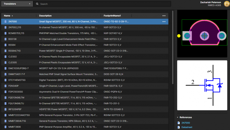
Store, share, and access your transistor parts data for your Altium Designer project through the Altium 365 platform.
When you need footprint transistor parts data for your PCBs, don’t use a 3rd party parts service. Altium Designer includes the tools you need to stay productive and find the parts you need. When you make the switch to Altium Designer, you’ll also have access to the industry’s best circuit board design tools in a single program.
Altium Designer on Altium 365 delivers unprecedented integration to the electronics industry until now relegated to the world of software development, allowing designers to work from home and reach unprecedented levels of efficiency.
We have only scratched the surface of what is possible to do with Altium Designer on Altium 365. You can check the product page for a more in-depth feature description or one of the On-Demand Webinars.


