Backdrill it Baby - How to Reduce Signal Distortions on Your PCB
Over the years, engineers have developed several approaches to deal with noises that can distort high speed digital signal integrity in printed circuit board backdrill designs. And as our designs push new boundaries, so does the complexity of our techniques to cope with new challenges. Today, the speed of digital design systems is in the GHz, a speed that creates more prominent challenges than the past. And with edge rates at the picoseconds, any impedance discontinuity, disturbance in inductance or parasitic capacitance can adversely affect signal integrity and quality. While there are various sources that can cause signal disturbances, one particular source, sometimes overlooked, is the via. Read on for more information on how to reduce PCB signal distortions.
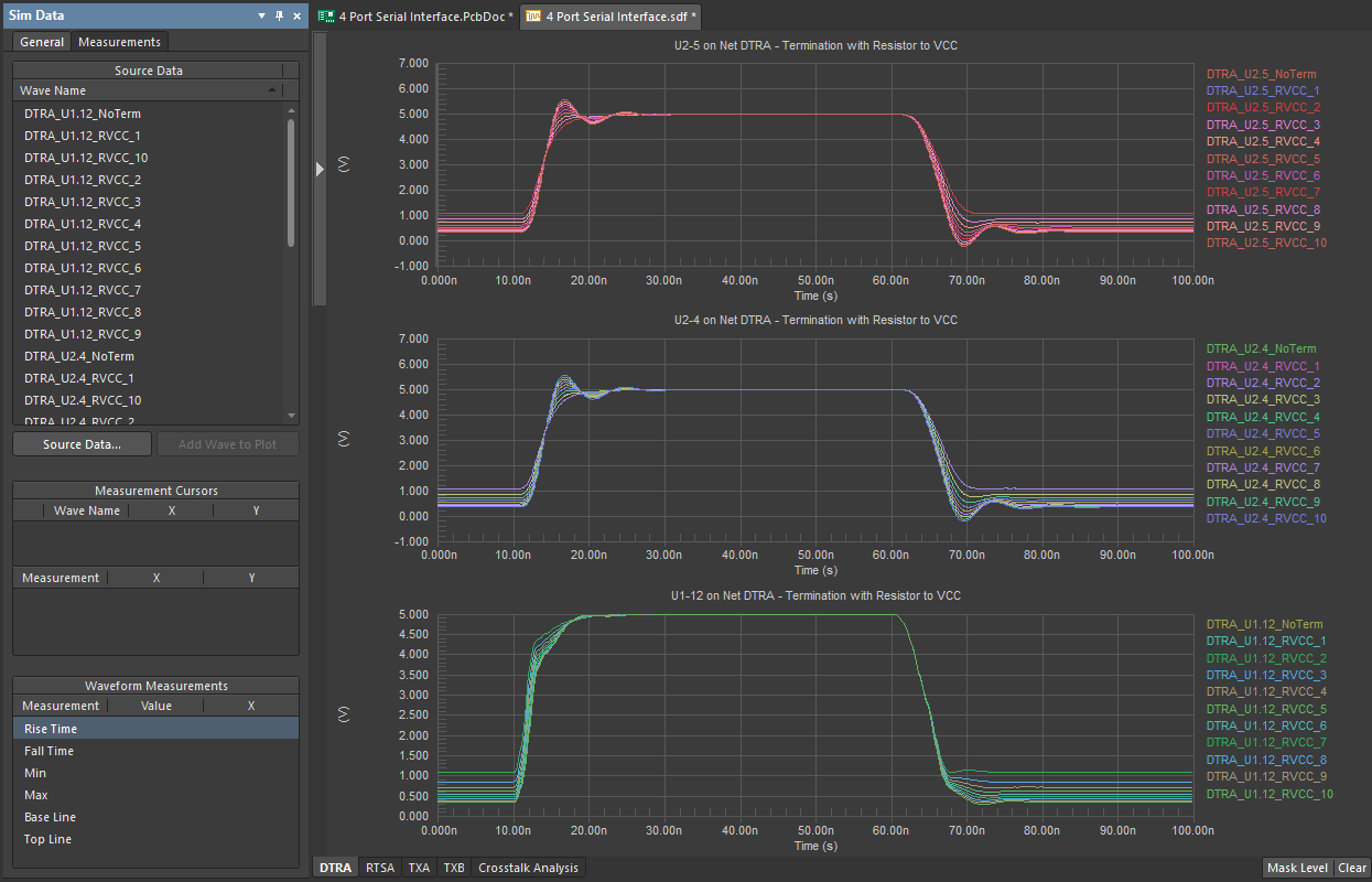
Vias signals, in High Density Interconnect (HDI), high layer-count printed boards, and thick backplanes/midplanes, can suffer from added jitter, attenuation, and higher bit error rates (BER) leading to data being misinterpreted at the receiver end.
Take for example backplanes and daughter cards. When it comes to impedance discontinuities, the focus with a circuit board is often the connectors between them and the motherboard. It’s usually the case that these connectors are very well matched in terms of impedance, and the actual source of discontinuity are the PCB design vias.
As data rates increase, the amount of distortion introduced by the Plated-through holes (PTH) via structures also increases – usually at an exponential rate considerably higher than the associated increase in data rate. For example, the distortion producing effects of a PTH via at a 6.25 Gb/s data rate is often more than double that at 3.125 Gb/s.
The presence of the unneeded stubs at the bottom and top that extend past their last connected layer make the vias appear as low impedance discontinuities. One way engineers overcome the extra capacitance of these vias is to minimize their lengths and therefore reduce their impedance. This is where backdrilling comes in.
Backing It Up with Backdrilling
Backdrilling has been used as a widely accepted, simple and effective method to minimize channel signal integrity by removing via stubs. This technique is referred to as Controlled Depth Drilling that uses conventional numerically controlled (NC) drill equipment. And this technique can be applied to any type of circuit board, not just thick ones like backplanes.
The backdrilling process involves using a drill bit slightly larger in diameter than the one used to create the original via hole to remove unneeded conductive stubs. This bit is usually 8 mils over the primary drill size, but many manufacturers can meet tighter specifications.
One has to remember that the trace and plane clearances need to be large enough, so the backdrilling procedure doesn’t drill through traces and planes close by the via being backdrilled. To avoid drilling through traces and planes it’s recommended to have a clearance of 10 mils.
In general, decreasing via stub lengths by backdrilling has many advantages, including:
-
Reducing deterministic jitter by orders of magnitude, resulting in lower BER.
-
Reducing signal attenuation due to improved impedance matching.
-
Reducing EMI/EMC radiation from the stub end and a channel bandwidth amplifier.
-
Reducing excitation of resonance modes and via-to-via crosstalk.
-
Minimizing design and layout impact with lower fabrication costs than sequential lamination.
Communicating Backdrilling Intent
As the use of the backdrilling technique becomes more frequently used in High Density Interconnect and High Speed Design applications, so are the reliability issues attributed to this practice. Some of the issues driving this include the lack of design guidelines, fabrication tolerances, and ensuring the design intent is well communicated to the manufacture within the fabrication package.
So how do you ensure your manufacturer has all the information needed for successfully back drilling all the target vias and PTH components on your circuit board? And how do you keep track of the multiple levels of back drilling specifications throughout your design?
What’s needed need is a simple, visual configuration tool, integrated into your design rules, that enables you to specify different back drilling configurations for selected objects. And after that, you can simply let the software do the work for you knowing which vias needs to be backdrilled. See how easy backdrilling can be in Altium Designer®.


