Die Kennzeichnung eines Lagenaufbaus
PDF herunterladen
A differential signaling system is one where a signal is transmitted down a pair of tightly coupled carriers, one of these carrying the signal, the other carrying an equal but opposite image of the signal. Differential signaling was developed to cater for situations where the logic reference ground of the signal source could not be well connected to the logic reference ground of the load. An…
With increasing device switching speeds, controlled impedance routing has become the hot topic for the digital designer. This article will discuss how you can use Altium Designer's Signal Integrity analysis engine to match component impedances, and the controlled impedance routing capabilities in the PCB editor. There is a saying bandied about in engineering circles - there are only two kinds of…
Parent page: The Routing Two of the core challenges with routing a high speed design are controlling the impedance of the routes, and matching the lengths of critical nets. Impedance controlled routing ensures that the signal that leaves an output pin is correctly received by the target input pins. Matching the route lengths ensures that timing-critical signals arrive at their target pins at the…
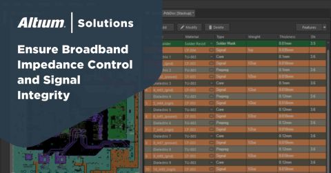
Related Videos Define New Layer Stacks Layer Stack Regions The PCB is designed and formed as a stack of layers. In the early days of printed circuit board (PCB) manufacturing, the board was simply an insulating core layer, clad with a thin layer of copper on one or both sides. Wiring was formed in the copper layer(s) as conductive traces, by etching away (removing) unwanted copper. A simple,…
The traditional approach to circuit board design has been to place the components on the top and bottom surfaces of the board. This process is well supported by circuit board assembly houses, which typically use automated pick and place machines to position each component, ready to be soldered onto the surface. The ever-increasing demand for smaller and more integrated electronic products,…
Parent page: Finalizing the Board Design Via stitching is a technique used to tie together larger copper areas on different layers, in effect creating a strong vertical connection through the board structure, helping maintain a low impedance and short return loops. Via stitching can also be used to tie areas of copper that might otherwise be isolated from their net, to that net. In RF designs, to…
How many of us got into electronics because we were drawn by the myriad of cool switches, knobs, lights and other suitably gadget-centric controls? Fast forward a good few years and that allure is still there, only it is now replaced with the "Snazzy GUI" factor - electronic products that have a sleek, sexy interface. Central to these ever-advancing (and shrinking) product interfaces is touch…
Understanding the Challenge This article does not attempt to provide a complete discussion of high speed design, for that there are a number of highly experienced and scholarly designers and engineers that have written excellent reference papers and books on the subject. Refer to the References section for links to these authors, and the papers used during research for this article. The purpose…
Additional Resources xSignals Enhanced Phase and Delay Tuning The Challenge With ever-increasing device switching speeds comes the challenge of maintaining the integrity of the signal, and meeting the signal's timing requirements. The signal integrity can be managed through controlled impedance routing, which is achieved though careful design of both the PCB stackup and the routing widths to be…
Controlled Depth Drilling (CDD), also known as back drilling, is a technique used to remove the unused portion, or stub, of copper barrel from a thru-hole in a printed circuit board. When a high-speed signal travels between PCB layers through a copper barrel, it can be distorted. If the signal layer usage results in a stub being present, and the stub is long, then that distortion can become…