Design for manufacturing (DFM) is the process for design engineers to review the design of a product to optimize its dimensions, materials, tolerances and functionality through the most efficient manufacturing means possible.
Your PCB assembler can offer intrusive soldering as an assembly option. Here’s how it works and what not to do to your PCB footprint.
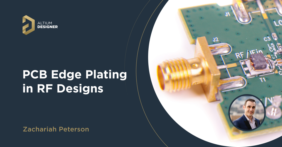
RF designs sometimes use PCB edge plating to contain electromagnetic fields and ruggedize a PCBA.
It’s often the case that PCB prototypes look nothing like a final product. If you’re transitioning from PCB prototype to volume production, learn more about optimizing your design.
Protect your PCB design from common assembly defects that arise in automated production processes. While the use of automated lines significantly reduces the likelihood of defects, issues like solder bridges, open joints, floating components, and warpage can still occur. - Learn about common PCB assembly defects and their causes to enhance your design process. - Discover techniques to inspect and mitigate defects in your PCB assembly. - Gain insights on ensuring the cleanliness and reliability of your assembled boards. By understanding these challenges and implementing design and fabrication best practices, you can minimize the chances of defects and improve the overall quality of your PCBs.
In this episode, we continue the discussion on diversifying the electronic supply chain. Our guest Case Engelen the CEO of Titoma shares his insight about moving some of the manufacturing to other Southeast Asian countries and South America.
Fabricators typically purchase flexible laminate, which consists of a layer of rolled annealed or electro-deposited copper on one of both sides of the dielectric. The most common dielectrics are polyimide, LCP, and polyester.
Outgassing from a PCB can occur during assembly, at high temperature, and in high vacuum. Make sure you follow these guidelines to reduce outgassing.